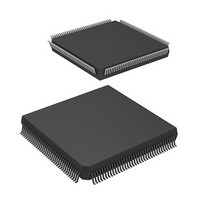
DF2338VFC25IV Renesas Electronics America, DF2338VFC25IV Datasheet - Page 463

DF2338VFC25IV
Manufacturer Part Number
DF2338VFC25IV
Description
MCU 3V 256K I-TEMP PB-FREE 144-Q
Manufacturer
Renesas Electronics America
Series
H8® H8S/2300r
Specifications of DF2338VFC25IV
Core Processor
H8S/2000
Core Size
16-Bit
Speed
25MHz
Connectivity
SCI, SmartCard
Peripherals
DMA, POR, PWM, WDT
Number Of I /o
106
Program Memory Size
256KB (256K x 8)
Program Memory Type
FLASH
Ram Size
8K x 8
Voltage - Supply (vcc/vdd)
2.7 V ~ 3.6 V
Data Converters
A/D 12x10b; D/A 4x8b
Oscillator Type
Internal
Operating Temperature
-40°C ~ 85°C
Package / Case
144-QFP
Lead Free Status / RoHS Status
Lead free / RoHS Compliant
Eeprom Size
-
- Current page: 463 of 1246
- Download datasheet (7Mb)
9.16.3
Port F pins also function as bus control signal input/output pins (AS, RD, HWR, LWR, LCAS,
BREQO, BREQ, and BACK) and the system clock (φ) output pin. The pin functions differ
between modes 4 to 6, and mode 7. Port F pin functions are shown in table 9.31.
Table 9.31 Port F Pin Functions
Pin
PF
PF
PF
PF
7
6
5
4
/φ
/AS
/RD
/HWR
Pin Functions
Selection Method and Pin Functions
The pin function is switched as shown below according to bit PF7DDR.
The pin function is switched as shown below according to the operating mode,
bit PF6DDR, and bit ASOD in PFCR2.
The pin function is switched as shown below according to the operating mode
and bit PF5DDR.
The pin function is switched as shown below according to the operating mode
and bit PF4DDR.
PF7DDR
Pin function
Operating
Mode
ASOD
PF6DDR
Pin function
Operating
Mode
PF5DDR
Pin function
Operating
Mode
PF4DDR
Pin function
AS output
HWR output pin
RD output pin
Modes 4 to 6
Modes 4 to 6
pin
—
0
PF
—
—
7
Modes 4 to 6
input pin
PF
0
6
pin
0
input
Rev.4.00 Sep. 07, 2007 Page 431 of 1210
1
PF
PF
PF
5
4
6
input pin
input pin
pin
output
1
0
0
Mode 7
Mode 7
PF
φ output pin
6
pin
0
input
REJ09B0245-0400
PF
PF
1
Mode 7
5
4
—
output pin
output pin
PF
1
1
6
pin
output
1
Related parts for DF2338VFC25IV
Image
Part Number
Description
Manufacturer
Datasheet
Request
R

Part Number:
Description:
KIT STARTER FOR M16C/29
Manufacturer:
Renesas Electronics America
Datasheet:

Part Number:
Description:
KIT STARTER FOR R8C/2D
Manufacturer:
Renesas Electronics America
Datasheet:

Part Number:
Description:
R0K33062P STARTER KIT
Manufacturer:
Renesas Electronics America
Datasheet:

Part Number:
Description:
KIT STARTER FOR R8C/23 E8A
Manufacturer:
Renesas Electronics America
Datasheet:

Part Number:
Description:
KIT STARTER FOR R8C/25
Manufacturer:
Renesas Electronics America
Datasheet:

Part Number:
Description:
KIT STARTER H8S2456 SHARPE DSPLY
Manufacturer:
Renesas Electronics America
Datasheet:

Part Number:
Description:
KIT STARTER FOR R8C38C
Manufacturer:
Renesas Electronics America
Datasheet:

Part Number:
Description:
KIT STARTER FOR R8C35C
Manufacturer:
Renesas Electronics America
Datasheet:

Part Number:
Description:
KIT STARTER FOR R8CL3AC+LCD APPS
Manufacturer:
Renesas Electronics America
Datasheet:

Part Number:
Description:
KIT STARTER FOR RX610
Manufacturer:
Renesas Electronics America
Datasheet:

Part Number:
Description:
KIT STARTER FOR R32C/118
Manufacturer:
Renesas Electronics America
Datasheet:

Part Number:
Description:
KIT DEV RSK-R8C/26-29
Manufacturer:
Renesas Electronics America
Datasheet:

Part Number:
Description:
KIT STARTER FOR SH7124
Manufacturer:
Renesas Electronics America
Datasheet:

Part Number:
Description:
KIT STARTER FOR H8SX/1622
Manufacturer:
Renesas Electronics America
Datasheet:

Part Number:
Description:
KIT DEV FOR SH7203
Manufacturer:
Renesas Electronics America
Datasheet:


