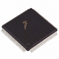
DSP56F826BU80 Freescale Semiconductor, DSP56F826BU80 Datasheet - Page 24

DSP56F826BU80
Manufacturer Part Number
DSP56F826BU80
Description
IC DSP 80MHZ 31.5K FLASH 100LQFP
Manufacturer
Freescale Semiconductor
Series
56F8xxr
Datasheet
1.DSP56F826BU80E.pdf
(56 pages)
Specifications of DSP56F826BU80
Core Processor
56800
Core Size
16-Bit
Speed
80MHz
Connectivity
EBI/EMI, SCI, SPI, SSI
Peripherals
POR, WDT
Number Of I /o
46
Program Memory Size
67KB (33.5K x 16)
Program Memory Type
FLASH
Ram Size
4.5K x 16
Voltage - Supply (vcc/vdd)
2.25 V ~ 2.75 V
Oscillator Type
External
Operating Temperature
-40°C ~ 85°C
Package / Case
100-LQFP
Lead Free Status / RoHS Status
Contains lead / RoHS non-compliant
Eeprom Size
-
Data Converters
-
Available stocks
Company
Part Number
Manufacturer
Quantity
Price
Company:
Part Number:
DSP56F826BU80
Manufacturer:
MOTOLOLA
Quantity:
853
Company:
Part Number:
DSP56F826BU80
Manufacturer:
Freescale Semiconductor
Quantity:
10 000
Part Number:
DSP56F826BU80
Manufacturer:
FREESCALE
Quantity:
20 000
Company:
Part Number:
DSP56F826BU80E
Manufacturer:
Freescale Semiconductor
Quantity:
10 000
Part Number:
DSP56F826BU80E
Manufacturer:
FREESCALE
Quantity:
20 000
V
supply (2.5V) from the voltage generated by the 3.3V V
rising faster than V
V
Typically this situation is avoided by using external discrete diodes in series between supplies, as shown
in
approximately 1.4, causing V
operation, the difference between supplies will typically be 0.8V and conduction through the diode chain
reduces to essentially leakage current. During supply sequencing, the following general relationship
should be adhered to:
V
In practice, V
3.4 AC Electrical Characteristics
Timing waveforms in
table. The levels of V
Figure 3-5
24
DD
DD
DDIO
Figure
•
•
•
•
should not be allowed to rise early (1). This is usually avoided by running the regulator for the V
should not rise so late that a large voltage difference is allowed between the two supplies (2).
Input Signal
Note: The midpoint is V
> V
Active state, when a bus or signal is driven, and enters a low impedance state
Tri-stated, when a bus or signal is placed in a high impedance state
Data Valid state, when a signal level has reached V
Data Invalid state, when a signal level is in transition between V
Supply
3-3. The series diodes forward bias when the difference between V
DD
shows the definitions of the following signal states:
DDA
> (V
is typically connected directly to V
Figure 3-3 Example Circuit to Control Supply Sequencing
Regulator
DDIO
DDIO
3.3V
IH
Section 3.4
Figure 3-4 Input Signal Measurement References
and V
.
- 1.4V)
Fall Time
IL
+ (V
Midpoint1
IL
DD
for an input signal are shown in
IH
V
are tested using the V
– V
to rise as V
IH
IL
)/2.
56F826 Technical Data, Rev. 14
DDIO
Regulator
Low
V
2.5V
IL
ramps up. When the V
DDIO
OL
IL
DDIO
and V
Pulse Width
or V
with some filtering.
supply, see
OH
IH
Figure
levels specified in the DC Characteristics
OL
Rise Time
and V
Figure
3-4.
High
OH
DD
3-3. This keeps V
V
regulator begins proper
DDIO,
DDIO
Freescale Semiconductor
V
V
90%
DD
and V
50%
DDA
10%
DD
DD
reaches
from
DD


