DSP56F826BU80 Freescale Semiconductor, DSP56F826BU80 Datasheet - Page 22
DSP56F826BU80
Manufacturer Part Number
DSP56F826BU80
Description
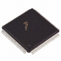
IC DSP 80MHZ 31.5K FLASH 100LQFP
Manufacturer
Freescale Semiconductor
Series
56F8xxr
Datasheet
1.DSP56F826BU80E.pdf
(56 pages)
Specifications of DSP56F826BU80
Core Processor
56800
Core Size
16-Bit
Speed
80MHz
Connectivity
EBI/EMI, SCI, SPI, SSI
Peripherals
POR, WDT
Number Of I /o
46
Program Memory Size
67KB (33.5K x 16)
Program Memory Type
FLASH
Ram Size
4.5K x 16
Voltage - Supply (vcc/vdd)
2.25 V ~ 2.75 V
Oscillator Type
External
Operating Temperature
-40°C ~ 85°C
Package / Case
100-LQFP
Lead Free Status / RoHS Status
Contains lead / RoHS non-compliant
Eeprom Size
-
Data Converters
-
Available stocks
Company
Part Number
Manufacturer
Quantity
Price
Company:

Part Number:
DSP56F826BU80
Manufacturer:
MOTOLOLA
Quantity:
853
Company:
Part Number:
DSP56F826BU80
Manufacturer:
Freescale Semiconductor
Quantity:
10 000
Part Number:
DSP56F826BU80
Manufacturer:
FREESCALE
Quantity:
20 000
Company:
Part Number:
DSP56F826BU80E
Manufacturer:
Freescale Semiconductor
Quantity:
10 000
Part Number:
DSP56F826BU80E
Manufacturer:
FREESCALE
Quantity:
20 000


22
1.
Input capacitance
Output capacitance
V
Low Voltage Interrupt, V
Low Voltage Interrupt, V
Power on Reset
Operating Conditions:
1. Schmitt Trigger inputs are: EXTBOOT, IRQA, IRQB, RESET, TCS, TCK, TRST, TMS, TDI and RXD1
2. Analog inputs are: ANA[0:7], XTAL and EXTAL. Specification assumes ADC is not sampling.
3. PWM pin output source current measured with 50% duty cycle.
4. PWM pin output sink current measured with 50% duty cycle.
5. I
6. Run (operating) I
inputs; measured with all modules enabled.
7. Wait I
less than 50pF on all outputs. C
measured with PLL enabled.
8. This low-voltage interrupt monitors the V
of the device is guaranteed under transient conditions when V
the V
9. This low-voltage interrupt monitors theV
the device is guaranteed under transient conditions when V
V
10. Power
active for as long as V
DD
EIC
supply current
DDT
interrupt is generated).
EIO
Wait
Stop
Run
interrupt is generated).
= I
DD
–
7
DD
6
on reset occurs whenever the V
measured using external square wave clock source (f
+ I
10
DDA
DD
(Total supply current for V
DD
V
Table 3-4 DC Electrical Characteristics (Continued)
SSIO
measured using 4MHz clock source. All inputs 0.2V from rail; outputs unloaded. All ports configured as
is below V
Characteristic
DDIO
DD
=V
power supply
SS
power supply
L
= V
= 20pF on EXTAL; all ports configured as inputs; EXTAL capacitance linearly affects wait I
POR
SSA
no matter how long the ramp-up rate is.
= 0V, V
DD
DDIO
DD
9
8
power supply. If V
56F826 Technical Data, Rev. 14
power supply drops below V
DD
DDA
power supply. If V
+ V
=V
DDA
DDIO
)
DD
=3.0–3.6V, V
DDIO
>V
DDIO
EIC
>V
osc
DDIO
EIO
(between the minimum specified V
drops below V
= 4MHz) into XTAL; all inputs 0.2V from rail; no DC loads;
(between the minimum specified V
drops below V
DD
= 2.25–2.75V, T
Symbol
POR
C
I
V
V
V
DDT
C
POR
OUT
EIO
EIC
IN
. While power is ramping up, this signal remains
5
EIC
EIO
, an interrupt is generated. Functionality of
, an interrupt is generated. Functionality
A
= –40° to +85°C, C
Min
2.4
2.0
—
—
—
—
—
—
DD
DDIO
Typ
and the point when the
2.7
2.2
1.7
12
47
21
8
2
Freescale Semiconductor
L
and the point when
≤ 50pF, f
Max
3.0
2.4
2.0
75
36
—
—
8
op
= 80MHz
DD
Unit
mA
mA
mA
pF
pF
;
V
V
V
Related parts for DSP56F826BU80
Image
Part Number
Description
Manufacturer
Datasheet
Request
R

Part Number:
Description:
Manufacturer:
Freescale Semiconductor, Inc
Datasheet:
Part Number:
Description:
Manufacturer:
Freescale Semiconductor, Inc
Datasheet:
Part Number:
Description:
Manufacturer:
Freescale Semiconductor, Inc
Datasheet:
Part Number:
Description:
Manufacturer:
Freescale Semiconductor, Inc
Datasheet:
Part Number:
Description:
Manufacturer:
Freescale Semiconductor, Inc
Datasheet:
Part Number:
Description:
Manufacturer:
Freescale Semiconductor, Inc
Datasheet:
Part Number:
Description:
Manufacturer:
Freescale Semiconductor, Inc
Datasheet:
Part Number:
Description:
Manufacturer:
Freescale Semiconductor, Inc
Datasheet:
Part Number:
Description:
Manufacturer:
Freescale Semiconductor, Inc
Datasheet:
Part Number:
Description:
Manufacturer:
Freescale Semiconductor, Inc
Datasheet:
Part Number:
Description:
Manufacturer:
Freescale Semiconductor, Inc
Datasheet:
Part Number:
Description:
Manufacturer:
Freescale Semiconductor, Inc
Datasheet:
Part Number:
Description:
Manufacturer:
Freescale Semiconductor, Inc
Datasheet:
Part Number:
Description:
Manufacturer:
Freescale Semiconductor, Inc
Datasheet:
Part Number:
Description:
Manufacturer:
Freescale Semiconductor, Inc
Datasheet: