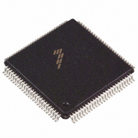
DSP56F826BU80 Freescale Semiconductor, DSP56F826BU80 Datasheet - Page 17

DSP56F826BU80
Manufacturer Part Number
DSP56F826BU80
Description
IC DSP 80MHZ 31.5K FLASH 100LQFP
Manufacturer
Freescale Semiconductor
Series
56F8xxr
Datasheet
1.DSP56F826BU80E.pdf
(56 pages)
Specifications of DSP56F826BU80
Core Processor
56800
Core Size
16-Bit
Speed
80MHz
Connectivity
EBI/EMI, SCI, SPI, SSI
Peripherals
POR, WDT
Number Of I /o
46
Program Memory Size
67KB (33.5K x 16)
Program Memory Type
FLASH
Ram Size
4.5K x 16
Voltage - Supply (vcc/vdd)
2.25 V ~ 2.75 V
Oscillator Type
External
Operating Temperature
-40°C ~ 85°C
Package / Case
100-LQFP
Lead Free Status / RoHS Status
Contains lead / RoHS non-compliant
Eeprom Size
-
Data Converters
-
Available stocks
Company
Part Number
Manufacturer
Quantity
Price
Company:
Part Number:
DSP56F826BU80
Manufacturer:
MOTOLOLA
Quantity:
853
Company:
Part Number:
DSP56F826BU80
Manufacturer:
Freescale Semiconductor
Quantity:
10 000
Part Number:
DSP56F826BU80
Manufacturer:
FREESCALE
Quantity:
20 000
Company:
Part Number:
DSP56F826BU80E
Manufacturer:
Freescale Semiconductor
Quantity:
10 000
Part Number:
DSP56F826BU80E
Manufacturer:
FREESCALE
Quantity:
20 000
Freescale Semiconductor
EXTBOOT
Table 2-1 56F826 Signal and Package Information for the 100 Pin LQFP (Continued)
RESET
Signal
Name
IRQA
IRQB
Pin No.
32
33
45
25
(Schmitt)
(Schmitt)
(Schmitt)
(Schmitt)
Type
Input
Input
Input
Input
External Interrupt Request A—The IRQA input is a synchronized external
interrupt request that indicates that an external device is requesting service. It
can be programmed to be level-sensitive or negative-edge-triggered. If
level-sensitive triggering is selected, an external pull-up resistor is required for
wired-OR operation.
If the processor is in the Stop state and IRQA is asserted, the processor will exit
the Stop state.
External Interrupt Request B—The IRQB input is an external interrupt request
that indicates that an external device is requesting service. It can be
programmed to be level-sensitive or negative-edge-triggered. If level-sensitive
triggering is selected, an external pull-up resistor is required for wired-OR
operation.
Reset—This input is a direct hardware reset on the processor. When RESET is
asserted low, the device is initialized and placed in the Reset state. A Schmitt
trigger input is used for noise immunity. When the RESET pin is deasserted, the
initial chip operating mode is latched from the external boot pin. The internal
reset signal will be deasserted synchronous with the internal clocks, after a fixed
number of internal clocks.
To ensure complete hardware reset, RESET and TRST should be asserted
together. The only exception occurs in a debugging environment when a
hardware device reset is required and it is necessary not to reset the
OnCE/JTAG module. In this case, assert RESET, but do not assert TRST.
External Boot—This input is tied to V
memory. Otherwise, it is tied to ground.
56F826 Technical Data, Rev. 14
Description
DD
to force device to boot from off-chip
Signals and Package Information
17


