DSP56F826BU80 Freescale Semiconductor, DSP56F826BU80 Datasheet - Page 16
DSP56F826BU80
Manufacturer Part Number
DSP56F826BU80
Description
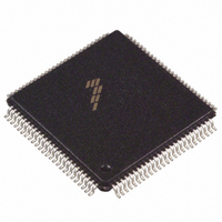
IC DSP 80MHZ 31.5K FLASH 100LQFP
Manufacturer
Freescale Semiconductor
Series
56F8xxr
Datasheet
1.DSP56F826BU80E.pdf
(56 pages)
Specifications of DSP56F826BU80
Core Processor
56800
Core Size
16-Bit
Speed
80MHz
Connectivity
EBI/EMI, SCI, SPI, SSI
Peripherals
POR, WDT
Number Of I /o
46
Program Memory Size
67KB (33.5K x 16)
Program Memory Type
FLASH
Ram Size
4.5K x 16
Voltage - Supply (vcc/vdd)
2.25 V ~ 2.75 V
Oscillator Type
External
Operating Temperature
-40°C ~ 85°C
Package / Case
100-LQFP
Lead Free Status / RoHS Status
Contains lead / RoHS non-compliant
Eeprom Size
-
Data Converters
-
Available stocks
Company
Part Number
Manufacturer
Quantity
Price
Company:

Part Number:
DSP56F826BU80
Manufacturer:
MOTOLOLA
Quantity:
853
Company:
Part Number:
DSP56F826BU80
Manufacturer:
Freescale Semiconductor
Quantity:
10 000
Part Number:
DSP56F826BU80
Manufacturer:
FREESCALE
Quantity:
20 000
Company:
Part Number:
DSP56F826BU80E
Manufacturer:
Freescale Semiconductor
Quantity:
10 000
Part Number:
DSP56F826BU80E
Manufacturer:
FREESCALE
Quantity:
20 000


16
(GPIOF6)
(GPIOF7)
(SCLK0)
Table 2-1 56F826 Signal and Package Information for the 100 Pin LQFP (Continued)
(MOSI0)
(MISO0)
Signal
Name
RXD0
RXD1
MISO
TXD0
TXD1
(SS0)
SS
Pin No.
86
87
97
96
93
92
Input/Output
Input/Output
Input/Output
Input/Output
Input/Output
Input/Output
(Schmitt)
Output
Output
Type
Input
Input
Input
Input
SPI Master In/Slave Out (MISO)—This serial data pin is an input to a master
device and an output from a slave device. The MISO line of a slave device is
placed in the high-impedance state if the slave device is not selected.
Port F GPIO—This General Purpose I/O (GPIO) pin can be individually
programmed as input or output.
After reset, the default state is MISO.
SPI Slave Select—In master mode, this pin is used to arbitrate multiple masters.
In slave mode, this pin is used to select the slave.
Port F GPIO—This General Purpose I/O (GPIO) pin can be individually
programmed as input or output.
After reset, the default state is SS.
Transmit Data (TXD0)—transmit data output
SPI Serial Clock—In master mode, this pin serves as an output, clocking slaved
listeners. In slave mode, this pin serves as the data clock input.
After reset, the default state is SCI output.
Receive Data (RXD0)— receive data input
SPI Master Out/Slave In—This serial data pin is an output from a master
device, and an input to a slave device. The master device places data on the
MOSI line one half-cycle before the clock edge the slave device uses to latch the
data.
After reset, the default state is SCI input.
Transmit Data (TXD1)—transmit data output
SPI Master In/Slave Out—This serial data pin is an input to a master device and
an output from a slave device. The MISO line of a slave device is placed in the
high-impedance state if the slave device is not selected.
After reset, the default state is SCI output.
Receive Data (RXD1)— receive data input
SPI Slave Select—In master mode, this pin is used to arbitrate multiple masters.
In slave mode, this pin is used to select the slave.
After reset, the default state is SCI input.
56F826 Technical Data, Rev. 14
Description
Freescale Semiconductor
Related parts for DSP56F826BU80
Image
Part Number
Description
Manufacturer
Datasheet
Request
R

Part Number:
Description:
Manufacturer:
Freescale Semiconductor, Inc
Datasheet:
Part Number:
Description:
Manufacturer:
Freescale Semiconductor, Inc
Datasheet:
Part Number:
Description:
Manufacturer:
Freescale Semiconductor, Inc
Datasheet:
Part Number:
Description:
Manufacturer:
Freescale Semiconductor, Inc
Datasheet:
Part Number:
Description:
Manufacturer:
Freescale Semiconductor, Inc
Datasheet:
Part Number:
Description:
Manufacturer:
Freescale Semiconductor, Inc
Datasheet:
Part Number:
Description:
Manufacturer:
Freescale Semiconductor, Inc
Datasheet:
Part Number:
Description:
Manufacturer:
Freescale Semiconductor, Inc
Datasheet:
Part Number:
Description:
Manufacturer:
Freescale Semiconductor, Inc
Datasheet:
Part Number:
Description:
Manufacturer:
Freescale Semiconductor, Inc
Datasheet:
Part Number:
Description:
Manufacturer:
Freescale Semiconductor, Inc
Datasheet:
Part Number:
Description:
Manufacturer:
Freescale Semiconductor, Inc
Datasheet:
Part Number:
Description:
Manufacturer:
Freescale Semiconductor, Inc
Datasheet:
Part Number:
Description:
Manufacturer:
Freescale Semiconductor, Inc
Datasheet:
Part Number:
Description:
Manufacturer:
Freescale Semiconductor, Inc
Datasheet: