SAF-XC886CLM-8FFI 5V AC Infineon Technologies, SAF-XC886CLM-8FFI 5V AC Datasheet - Page 121
SAF-XC886CLM-8FFI 5V AC
Manufacturer Part Number
SAF-XC886CLM-8FFI 5V AC
Description
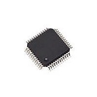
IC MCU 8BIT FLASH TQFP-48
Manufacturer
Infineon Technologies
Series
XC8xxr
Datasheet
1.SAF-XC888CLM-6FFA_5V_AC.pdf
(144 pages)
Specifications of SAF-XC886CLM-8FFI 5V AC
Program Memory Type
FLASH
Program Memory Size
32KB (32K x 8)
Package / Case
48-TFQFP
Core Processor
XC800
Core Size
8-Bit
Speed
103.2MHz
Connectivity
CAN, LIN, SSI, UART/USART
Peripherals
Brown-out Detect/Reset, POR, PWM, WDT
Number Of I /o
34
Ram Size
1.75K x 8
Voltage - Supply (vcc/vdd)
4.5 V ~ 5.5 V
Data Converters
A/D 8x10b
Oscillator Type
Internal
Operating Temperature
-40°C ~ 85°C
Data Bus Width
8 bit
Data Ram Size
1.75 KB
Interface Type
JTAG/SPI/SSC/UART
Maximum Clock Frequency
24 MHz
Number Of Programmable I/os
48
Number Of Timers
4
Operating Supply Voltage
5 V
Maximum Operating Temperature
+ 85 C
Mounting Style
SMD/SMT
Minimum Operating Temperature
- 40 C
On-chip Adc
8-ch x 10-bit
Lead Free Status / RoHS Status
Contains lead / RoHS non-compliant
For Use With
MCBXC88X - BOARD EVAL FOR INFINEON XC88X
Eeprom Size
-
Lead Free Status / Rohs Status
Lead free / RoHS Compliant
Other names
FX886CLM8FFI5VACXT
SAF-XC886CLM-8FFI AB
SAF-XC886CLM-8FFI AB
SAFXC886CLM8FFIABT
SP000217341
SAF-XC886CLM-8FFI AB
SAF-XC886CLM-8FFI AB
SAFXC886CLM8FFIABT
SP000217341


Table 38
Parameter
Input high voltage at
XTAL1
Pull-up current
Pull-down current
Input leakage current
Input current at XTAL1
Overload current on any
pin
Absolute sum of
overload currents
Voltage on any pin
during
Maximum current per
pin (excluding
V
Maximum current for all
pins (excluding
and
Maximum current into
V
Maximum current out of
V
1) Not subjected to production test, verified by design/characterization. Hysteresis is implemented to avoid meta
2) An additional error current (
3) Not subjected to production test, verified by design/characterization.
4) Not subjected to production test, verified by design/characterization. However, for applications with strict low
Data Sheet
SS
DDP
SS
stable states and switching due to internal ground bounce. It cannot be guaranteed that it suppresses
switching due to external system noise.
RESET pin have internal pull devices and are not included in the input leakage current characteristic.
power-down current requirements, it is mandatory that no active voltage source is supplied at any GPIO pin
when
)
V
SS
V
V
)
DDP
DDP
is powered off.
power off
Input/Output Characteristics (Operating Conditions apply) (cont’d)
V
V
DDP
DDP
and
I
INJ
Symbol
V
I
I
I
I
I
Σ|
V
I
Σ|
I
I
PU
PD
OZ1
ILX
OV
M
MVDDP
MVSS
IHX
PO
) will flow if an overload current flows through an adjacent pin. TMS pin and
I
I
OV
M
SR SR –
|
|
SR 0.7 ×
SR –
SR –
CC -1
CC - 10
SR -5
SR –
SR –
SR –
SR –
SR –
min.
V
-50
50
Limit Values
DDC
114
max.
V
0.5
-5
–
5
–
1
10
5
25
0.3
15
90
120
120
DDC
+
Unit Test Conditions
V
µA
µA
µA
µA
µA
µA
mA
mA
V
mA
mA
mA
mA
V
V
V
V
0 <
T
3)
4)
3)
3)
A
IHP,min
ILP,max
ILP,max
IHP,min
Electrical Parameters
≤ 125°C
V
IN
XC886/888CLM
<
V
DDP
2)
V1.2, 2009-07
,
Related parts for SAF-XC886CLM-8FFI 5V AC
Image
Part Number
Description
Manufacturer
Datasheet
Request
R

Part Number:
Description:
IC MCU 8BIT FLASH 48-TQFP
Manufacturer:
Infineon Technologies
Datasheet:

Part Number:
Description:
IC MCU 8BIT FLASH 48-TQFP
Manufacturer:
Infineon Technologies
Datasheet:
Part Number:
Description:
8-bit Microcontrollers - MCU MICROCONTROLLER 8-BIT
Manufacturer:
Infineon Technologies
Part Number:
Description:
IC MCU 8BIT FLASH 48-TQFP
Manufacturer:
Infineon Technologies
Datasheet:
Part Number:
Description:
IC MCU 8BIT FLASH TQFP-48
Manufacturer:
Infineon Technologies
Datasheet:
Part Number:
Description:
IC MCU 8BIT FLASH 48-TQFP
Manufacturer:
Infineon Technologies
Datasheet:
Part Number:
Description:
IC MCU 8BIT FLASH 48-TQFP
Manufacturer:
Infineon Technologies
Datasheet:
Part Number:
Description:
IC MCU 8BIT FLASH 48-TQFP
Manufacturer:
Infineon Technologies
Datasheet:
Part Number:
Description:
8-bit Microcontrollers - MCU
Manufacturer:
Infineon Technologies
Part Number:
Description:
8-bit Microcontrollers - MCU
Manufacturer:
Infineon Technologies
Part Number:
Description:
8-bit Microcontrollers - MCU
Manufacturer:
Infineon Technologies
Part Number:
Description:
8-bit Microcontrollers - MCU MICROCONTROLLER 8-BIT
Manufacturer:
Infineon Technologies

Part Number:
Description:
Manufacturer:
Infineon Technologies AG
Datasheet:
Part Number:
Description:
Manufacturer:
Infineon Technologies AG
Datasheet:
Part Number:
Description:
Manufacturer:
Infineon Technologies AG
Datasheet: