M38039G4HSP#U0 Renesas Electronics America, M38039G4HSP#U0 Datasheet
M38039G4HSP#U0
Specifications of M38039G4HSP#U0


Related parts for M38039G4HSP#U0


M38039G4HSP#U0 Summary of contents
Page 1
To our customers, Old Company Name in Catalogs and Other Documents st On April 1 , 2010, NEC Electronics Corporation merged with Renesas Technology Corporation, and Renesas Electronics Corporation took over all the business of both companies. Therefore, although the ...
Page 2
All information included in this document is current as of the date this document is issued. Such information, however, is subject to change without any prior notice. Before purchasing or using any Renesas Electronics products listed herein, please confirm ...
Page 3
Group (Spec.H QzROM version) SINGLE-CHIP 8-BIT CMOS MICROCOMPUTER DESCRIPTION The 3803 group (Spec.H QzROM version) is the 8-bit microcomputer based on the 740 family core technology. The 3803 group (Spec.H QzROM version) is designed for household products, office automation ...
Page 4
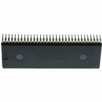
Group (Spec.H QzROM version) PIN CONFIGURATION (TOP VIEW RDY3 CLK3 / /DA 0 ...
Page 5
Group (Spec.H QzROM version) PIN CONFIGURATION (TOP VIEW) Fig 2. 3803 group (Spec.H QzROM version) pin configuration (PRDP0064BA-A) REJ03B0166-0113 Rev.1.13 Page 3 of 100 REF / ...
Page 6
Group (Spec.H QzROM version) PIN CONFIGURATION (TOP VIEW CLK3 / /AN 2 ...
Page 7
Group (Spec.H QzROM version) Table 1 Performance overview Parameter Number of basic instructions Minimum instruction execution time Oscillation frequency Memory sizes I/O port P0, P1, P2, P3, P4, P5, P6 Software pull-up resistors Interrupt Timer Serial interface PWM A/D ...
Page 8
Group (Spec.H QzROM version) Fig 4. Functional block diagram REJ03B0166-0113 Rev.1.13 Page 6 of 100 Aug 21, 2009 ...
Page 9
Group (Spec.H QzROM version) PIN DESCRIPTION Table 2 Pin description Pin Name Power source CC SS CNV CNV Reference REF voltage AV Analog power SS source Reset input RESET X Clock input IN ...
Page 10
Group (Spec.H QzROM version) PART NUMBERING Product name M3803 9 G Fig 5. Part numbering REJ03B0166-0113 Rev.1.13 Page 8 of 100 C H− XXX SP Package type SP : PRDP0064BA-A (64P4B PLQP0064KB-A (64P6Q- PLQP0064GA-A (64P6U-A) ...
Page 11
Group (Spec.H QzROM version) GROUP EXPANSION Renesas Technology expands the 3803 group (Spec.H QzROM version) as follows. Memory Type Support for QzROM version. Memory Expansion Plan ROM size (bytes) 48K 32K 24K 16K Fig 6. Memory expansion plan REJ03B0166-0113 ...
Page 12
Group (Spec.H QzROM version) Table 3 Support products QzROM size (bytes) Product name ROM size for User M38039G4H-XXXHP 16384 (16254) M38039G4H-XXXKP M38039G6H-XXXHP 24576 (24446) M38039G6H-XXXKP M38039G8H-XXXHP 32768 M38039G8H-XXXKP (32638) M38039GCH-XXXHP 49152 M38039GCH-XXXKP (49022) M38039GCH-XXXWG M38039G4HSP 16384 ...
Page 13
Group (Spec.H QzROM version) FUNCTIONAL DESCRIPTION CENTRAL PROCESSING UNIT (CPU) The 3803 group (Spec.H QzROM version) uses the standard 740 Family instruction set. Refer to the table of 740 Family addressing modes and machine instructions or the 740 Family ...
Page 14
Group (Spec.H QzROM version) Interrupt request Push Return M(S)←( Address on Stack (S)←(S) − 1 M(S)←( ← − Subroutine Execute RTS (S)←( POP Return Address from ...
Page 15
Group (Spec.H QzROM version) [Processor status register (PS)] The processor status register is an 8-bit register consisting of 5 flags which indicate the status of the processor after an arithmetic operation and 3 flags which decide MCU operation. Branch ...
Page 16
Group (Spec.H QzROM version) [CPU Mode Register (CPUM)] 003B The CPU mode register contains the stack page selection bit, the internal system clock control bits, etc. The CPU mode register is allocated at address 003B b7 Fig 9. Structure ...
Page 17
Group (Spec.H QzROM version) MISRG (1) Bit 0 of address 0010 : Oscillation stabilizing time 16 set after STP instruction released bit When the MCU stops the clock oscillation by the STP instruction and the STP instruction has been ...
Page 18
Group (Spec.H QzROM version) MEMORY • Special Function Register (SFR) Area The Special Function Register area in the zero page contains control registers such as I/O ports and timers. • RAM The RAM is used for data storage and ...
Page 19
Group (Spec.H QzROM version) Port P0 (P0) 0000 16 Port P0 direction register (P0D) 0001 16 Port P1 (P1) 0002 16 Port P1 direction register (P1D) 0003 16 Port P2 (P2) 0004 16 Port P2 direction register (P2D) 0005 ...
Page 20
Group (Spec.H QzROM version) I/O PORTS The I/O ports have direction registers which determine the input/output direction of each individual pin. Each bit in a direction register corresponds to one pin, and each pin can be set to be ...
Page 21
Group (Spec.H QzROM version) (1) Ports Pull-up control bit Direction register Port latch Data bus A/D converter input (3) Ports Pull-up control bit Direction register Data bus Port latch ...
Page 22
Group (Spec.H QzROM version) (9) Port P3 7 Pull-up control bit Serial I/O3 mode selection bit Serial I/O3 enable bit S output enable bit RDY3 Direction register Data bus Port latch Serial I/O3 ready output (11) Port P4 1 ...
Page 23
Group (Spec.H QzROM version) (15) Port P5 2 Pull-up control bit Serial I/O2 synchronous clock selection bit Serial I/O2 port selection bit Direction register Data bus Port latch Serial I/O2 clock output Serial I/O2 external clock input (17) Ports ...
Page 24
Group (Spec.H QzROM version Fig 16. Structure of port pull-up control register (1) REJ03B0166-0113 Rev.1.13 Page 22 of 100 Port P0 pull-up control register (PULL0: address 0FF0 ) 16 P0 pull-up control bit 0 0: ...
Page 25
Group (Spec.H QzROM version Fig 17. Structure of port pull-up control register (2) REJ03B0166-0113 Rev.1.13 Page 23 of 100 Port P2 pull-up control register (PULL2: address 0FF2 ) 16 P2 pull-up control bit 0 0: ...
Page 26
Group (Spec.H QzROM version Fig 18. Structure of port pull-up control register (3) REJ03B0166-0113 Rev.1.13 Page 24 of 100 Port P4 pull-up control register (PULL4: address 0FF4 ) 16 P4 pull-up control bit 0 0: ...
Page 27
Group (Spec.H QzROM version Fig 19. Structure of port pull-up control register (4) REJ03B0166-0113 Rev.1.13 Page 25 of 100 Port P6 pull-up control register (PULL6: address 0FF6 ) 16 P6 pull-up control bit pull-up ...
Page 28
Group (Spec.H QzROM version) Termination of unused pins • Termination of common pins I/O ports: Select an input port or an output port and follow each processing method. In addition recommended that related registers be overwritten periodically ...
Page 29
Group (Spec.H QzROM version) INTERRUPTS The 3803 group (Spec.H QzROM version) interrupts are vector interrupts with a fixed priority scheme, and generated by 16 sources among 21 sources: 8 external, 12 internal, and 1 software. The interrupt sources, vector ...
Page 30
Group (Spec.H QzROM version) Interrupt request bit Interrupt enable bit Interrupt disable flag (I) Fig 20. Interrupt control diagram • Interrupt Disable Flag The interrupt disable flag is assigned to bit 2 of the processor status register. This flag ...
Page 31
Group (Spec.H QzROM version Interrupt edge selection register (INTEDGE : address 003A INT interrupt edge selection bit 0 INT interrupt edge selection bit 1 Not used (returns “0” when read) INT interrupt edge selection bit 2 INT ...
Page 32
Group (Spec.H QzROM version) • Interrupt Request Generation, Acceptance, and Handling Interrupts have the following three phases. (i) Interrupt Request Generation An interrupt request is generated by an interrupt source (external interrupt signal input, timer underflow, etc.) and the ...
Page 33
Group (Spec.H QzROM version) φ SYNC RD WR Address bus Data bus SYNC : CPU operation code fetch cycle (This is an internal signal that cannot be observed from the external unit.) BL, BH: Vector address of each interrupt ...
Page 34
Group (Spec.H QzROM version) <Notes> The interrupt request bit may be set to “1” in the following cases. • When setting the external interrupt active edge Related bits: INT interrupt edge selection bit 0 (bit 0 of interrupt edge ...
Page 35
Group (Spec.H QzROM version) TIMERS 8-bit Timers The 3803 group (Spec.H QzROM version) has four 8-bit timers: timer 1, timer 2, timer X, and timer Y. The timer 1 and timer 2 use one prescaler in common, and the ...
Page 36
Group (Spec.H QzROM version) (4) Pulse Width Measurement Mode • Mode selection This mode can be selected by setting “11” to the timer X operating mode bits (bits 1 and 0) and the timer Y operating mode bits (bits ...
Page 37
Group (Spec.H QzROM version “00” (1/2, 1/4, 1/8, 1/16, 1/32, 1/64, 1/128, 1/256, 1/512, 1/1024) “11” Divider Count source selection bit “10” X CIN Main clock division ratio selection bits f(X ) CIN CNTR active 0 edge ...
Page 38
Group (Spec.H QzROM version) b7 Fig 26. Structure of timer XY mode register REJ03B0166-0113 Rev.1.13 Page 36 of 100 b0 Timer XY mode register (TM : address 0023 Timer X operating mode bits Timer mode ...
Page 39
Group (Spec.H QzROM version Fig 27. Structure of timer 12, X and timer Y, Z count source selection registers REJ03B0166-0113 Rev.1.13 Page 37 of 100 b0 Timer 12, X count source selection register (T12XCSS : address 000E ...
Page 40
Group (Spec.H QzROM version) 16-bit Timer The timer 16-bit timer. When the timer reaches “0000 ...
Page 41
Group (Spec.H QzROM version) (4) Pulse period measurement mode • Mode selection This mode can be selected by setting “010” to the timer Z operating mode bits (bits and setting “0” to the timer/event counter mode ...
Page 42
Group (Spec.H QzROM version) (6) Programmable waveform generating mode • Mode selection This mode can be selected by setting “100” to the timer Z operating mode bits (bits and setting “0” to the timer/event counter mode ...
Page 43
Group (Spec.H QzROM version) <Notes regarding all modes> • Timer Z write control Which write control can be selected by the timer Z write control bit (bit 3) of the timer Z mode register (address 002A data to both ...
Page 44
Group (Spec.H QzROM version Note: When selecting the modes except the timer/event counter mode, set “0” to this bit. Fig 29. Structure of timer Z mode register REJ03B0166-0113 Rev.1.13 Page 42 of 100 Timer Z mode register ...
Page 45
Group (Spec.H QzROM version) FFFF 16 TL 0000 16 Fig 30. Timing chart of timer/event counter mode FFFF TL 0000 Waveform output from CNTR pin 2 Fig 31. Timing chart of pulse output mode REJ03B0166-0113 Rev.1.13 Page 43 of ...
Page 46
Group (Spec.H QzROM version) 0000 FFFF 16 Signal input from CNTR pin 2 Fig 32. Timing chart of pulse period measurement mode (Measuring term between two rising edges) 0000 FFFF 16 ...
Page 47
Group (Spec.H QzROM version) FFFF 0000 Signal output from CNTR pin 2 Fig 34. Timing chart of programmable waveform generating mode FFFF Signal input from INT pin 1 Signal output from CNTR pin 2 Fig 35. Timing chart of ...
Page 48
Group (Spec.H QzROM version) SERIAL INTERFACE Serial I/O1 Serial I/O1 can be used as either clock synchronous or asynchronous (UART) serial I/O. A dedicated timer is also provided for baud rate generation ...
Page 49
Group (Spec.H QzROM version) (2) Asynchronous Serial I/O (UART) Mode Clock asynchronous serial I/O mode (UART) can be selected by clearing the serial I/O1 mode selection bit (b6) of the serial I/O1 control register to “0”. Eight serial data ...
Page 50
Group (Spec.H QzROM version) [Transmit Buffer Register 1/Receive Buffer Register 1 (TB1/RB1)] 0018 16 The transmit buffer register 1 and the receive buffer register 1 are located at the same address. The transmit buffer is write-only and the receive ...
Page 51
Group (Spec.H QzROM version) Serial I/O1 status register b7 b0 (SIO1STS : address 0019 Transmit buffer empty flag (TBE) 0: Buffer full 1: Buffer empty Receive buffer full flag (RBF) 0: Buffer empty 1: Buffer full Transmit shift completion ...
Page 52
Group (Spec.H QzROM version) <Notes concerning serial I/O1> 1. Notes when selecting clock synchronous serial I/O 1.1 Stop of transmission operation • Note Clear the serial I/O1 enable bit and the transmit enable bit to “0” (serial I/O and ...
Page 53
Group (Spec.H QzROM version output of reception side RDY1 • Note When signals are output from the S RDY1 side by using an external clock in the clock synchronous serial I/O mode, set all of the receive ...
Page 54
Group (Spec.H QzROM version) Serial I/O2 The serial I/O2 function can be used only for clock synchronous serial I/O. For clock synchronous serial I/O2, the transmitter and the receiver must use the same clock. If the internal clock is ...
Page 55
Group (Spec.H QzROM version) Transfer clock (Note 1) Serial I/O2 register write signal Serial I/O2 output S OUT2 Serial I/O2 input S IN2 Receive enable signal S RDY2 Notes1: When the internal clock is selected as the transfer clock, ...
Page 56
Group (Spec.H QzROM version) Serial I/O3 Serial I/O3 can be used as either clock synchronous or asynchronous (UART) serial I/O3. A dedicated timer is also provided for baud rate generation ...
Page 57
Group (Spec.H QzROM version) (2) Asynchronous Serial I/O (UART) Mode Clock asynchronous serial I/O mode (UART) can be selected by clearing the serial I/O3 mode selection bit (b6) of the serial I/O3 control register to “0”. Eight serial data ...
Page 58
Group (Spec.H QzROM version) [Transmit Buffer Register 3/Receive Buffer Register 3 (TB3/RB3)] 0030 16 The transmit buffer register 3 and the receive buffer register 3 are located at the same address. The transmit buffer is write-only and the receive ...
Page 59
Group (Spec.H QzROM version) Serial I/O3 status register b7 b0 (SIO3STS : address 0031 Transmit buffer empty flag (TBE) 0: Buffer full 1: Buffer empty Receive buffer full flag (RBF) 0: Buffer empty 1: Buffer full Transmit shift completion ...
Page 60
Group (Spec.H QzROM version) <Notes concerning serial I/O3> 1. Notes when selecting clock synchronous serial I/O 1.1 Stop of transmission operation • Note Clear the serial I/O3 enable bit and the transmit enable bit to “0” (serial I/O and ...
Page 61
Group (Spec.H QzROM version output of reception side RDY3 • Note When signals are output from the S RDY3 side by using an external clock in the clock synchronous serial I/O mode, set all of the receive ...
Page 62
Group (Spec.H QzROM version) PULSE WIDTH MODULATION (PWM) The 3803 group (Spec.H QzROM version) has PWM functions with an 8-bit resolution, based on a signal that is the clock input X or that clock input divided ...
Page 63
Group (Spec.H QzROM version) b7 Fig 51. Structure of PWM control register PWM output PWM register write signal PWM prescaler write signal When the contents of the PWM register or PWM prescaler have changed, the PWM output will change ...
Page 64
Group (Spec.H QzROM version) A/D CONVERTER [AD Conversion Register 1, 2] AD1, AD2 The AD conversion register is a read-only register that stores the result of an A/D conversion. When reading this register during an A/D conversion, the previous ...
Page 65
Group (Spec.H QzROM version) b7 AD/DA control register (Address 0034 ) Comparator /AN ...
Page 66
Group (Spec.H QzROM version) D/A CONVERTER The 3803 group (Spec.H QzROM version) has two internal D/A converters (DA and DA ) with 8-bit resolution The D/A conversion is performed by setting the value in each DAi conversion ...
Page 67
Group (Spec.H QzROM version) WATCHDOG TIMER The watchdog timer gives a mean of returning to the reset status when a program cannot run on a normal loop (for example, because of a software run-away). The watchdog timer consists of ...
Page 68
Group (Spec.H QzROM version) RESET CIRCUIT To reset the microcomputer, RESET pin should be held at an “L” level for 16 cycles or more Then the RESET pin is IN returned to an “H” level (the ...
Page 69
Group (Spec.H QzROM version) (1) Port P0 (P0) (2) Port P0 direction register (P0D) (3) Port P1 (P1) (4) Port P1 direction register (P1D) (5) Port P2 (P2) (6) Port P2 direction register (P2D) (7) Port P3 (P3) (8) ...
Page 70
Group (Spec.H QzROM version) CLOCK GENERATING CIRCUIT The 3803 group (Spec.H QzROM version) has two built-in oscillation circuits: main clock OUT sub clock X -X oscillation circuit. An oscillation circuit CIN COUT can be formed by ...
Page 71
Group (Spec.H QzROM version CIN COUT CIN COUT Notes : Insert a damping resistor if required. The resistance will vary depending on the oscillator and the oscillation drive capacity setting. Use ...
Page 72
Group (Spec.H QzROM version COUT CIN “0” “1” Port X C switch bit OUT Main clock division ratio selection bits (Note 1) (Note 4) Low-speed mode High-speed or middle-speed mode Main clock (X Q ...
Page 73
Group (Spec.H QzROM version) Reset Middle-speed mode CM (f(φ MHz) “1”←→”0” MHz oscillating (32 kHz stopped) 4 Middle-speed mode CM (f(φ MHz) “1”←→”0” ...
Page 74
Group (Spec.H QzROM version) QzROM Writing Mode In the QzROM writing mode, the user ROM area can be rewritten while the microcomputer is mounted on-board by using a serial programmer which is applicable for this microcomputer. Table 9 lists ...
Page 75
Group (Spec.H QzROM version RDY3 CLK3 / ...
Page 76
Group (Spec.H QzROM version ESPGMB P4 ESCLK ESDA V PP RESET * GND * Connect to oscillation circuit : QzROM pin Fig. 69 Pin connection diagram (M38039GXHSP) REJ03B0166-0113 Rev.1.13 Page 74 of 100 ...
Page 77
Group (Spec.H QzROM version) PIN CONFIGURATION (TOP VIEW /AN 6 CLK3 / ...
Page 78
Group (Spec.H QzROM version) T_VDD T_VPP T_TXD T_RXD T_SCLK T_BUSY T_PGM/OE/MD RESET circuit T_RESET GND Note: For the programming circuit, the wiring capacity of each signal pin must not exceed 47 pF. Fig. 71 When using programmer of Suisei ...
Page 79
Group (Spec.H QzROM version) Vcc *1: Open-collector buffer Note: For the programming circuit, the wiring capacity of each signal pin must not exceed 47 pF. ...
Page 80
Group (Spec.H QzROM version) NOTES NOTES ON PROGRAMMING 1. Processor Status Register (1) Initializing of processor status register Flags which affect program execution must be initialized after a reset. In particular essential to initialize the T and ...
Page 81
Group (Spec.H QzROM version) 6. Serial Interface In clock synchronous serial I/O, if the receive side is using an external clock and output the S RDY enable bit, the receive enable bit, and the S to ...
Page 82
Group (Spec.H QzROM version) (2) Connection of bypass capacitor across V line In order to stabilize the system operation and avoid the latch-up, connect an approximately 0.1 µF bypass capacitor across the V line and the V line as ...
Page 83
Group (Spec.H QzROM version) NOTES ON PERIPHERAL FUNCTIONS Notes on Input and Output Ports 1. Use in Stand-By State When using the MCU in stand-by state* consumption, do not leave the input level of an I/O port undefined. Be ...
Page 84
Group (Spec.H QzROM version) Notes on Interrupts 1. Change of relevant register settings When the setting of the following registers or bits is changed, the interrupt request bit may be set to “1”. When not requiring the interrupt occurrence ...
Page 85
Group (Spec.H QzROM version) Notes on 16-bit Timer (timer Z) 1. Pulse output mode • Set the double-function port of the CNTR output. 2. Pulse period measurement mode • Set the double-function port of the CNTR input. • A ...
Page 86
Group (Spec.H QzROM version) 2. Notes when selecting clock asynchronous serial I/O (1) Stop of transmission operation Clear the transmit enable bit to “0” (transmit disabled). The transmission operation does not stop by clearing the serial I/Oi enable bit ...
Page 87
Group (Spec.H QzROM version) 3. Clock frequency during A/D conversion The comparator consists of a capacity coupling, and a charge of the capacity will be lost if the clock frequency is too low. Thus, make sure the following during ...
Page 88
Group (Spec.H QzROM version) Notes on Using Stop Mode • Register setting Since values of the prescaler 12 and Timer 1 are automatically reloaded when returning from the stop mode, set them again, respectively. (When the oscillation stabilizing time ...
Page 89
Group (Spec.H QzROM version) Notes On QzROM Writing Orders When ordering the QzROM product shipped after writing, submit the mask file (extension: .msk) which is made by the mask file converter MM. • Be sure to set the ROM ...
Page 90
Group (Spec.H QzROM version) ELECTRICAL CHARACTERISTICS Absolute maximum ratings Table 10 Absolute maximum ratings Symbol Parameter V Power source voltages CC V Input voltage Input voltage P3 ...
Page 91
Group (Spec.H QzROM version) Recommended operating conditions Table 11 Recommended operating conditions ( 1 Symbol Parameter V Power source When start oscillating CC (1) voltage High-speed mode f( φ ...
Page 92
Group (Spec.H QzROM version) Table 12 Recommended operating conditions ( 1 Symbol Σ I “H” total peak output current OH(peak) Σ I “H” total peak output current OH(peak) Σ I “L” ...
Page 93
Group (Spec.H QzROM version) Electrical characteristics Table 13 Electrical characteristics ( 1 Symbol Parameter V (1) “H” output voltage ...
Page 94
Group (Spec.H QzROM version) Table 14 Electrical characteristics ( 1 – °C, f(X CC Output transistors “off”, AD converter not operated) Symbol Parameter I Power source High-speed CC current mode ...
Page 95
Group (Spec.H QzROM version) A/D converter characteristics Table 15 A/D converter recommended operating conditions (V = 2 Symbol Parameter V Power source voltage CC (When A/D converter is used) V Analog convert reference ...
Page 96
Group (Spec.H QzROM version) Timing requirements and switching characteristics Table 18 Timing requirements ( 2 Symbol t (RESET) Reset input “L” pulse width Main clock X C ...
Page 97
Group (Spec.H QzROM version) Table 19 Timing requirements ( 2 Symbol Serial I/O1, serial I/O3 C CLK1 CLK3 clock input cycle time t (S ...
Page 98
Group (Spec.H QzROM version) Table 20 Switching characteristics ( 2 Symbol Parameter Serial I/O1, serial I/O3 WH CLK1 clock output “H” pulse WH CLK3 width ...
Page 99
Group (Spec.H QzROM version) Table 21 Switching characteristics ( 2 Symbol Parameter Serial I/O2 f CLK2 fall time of clock output t (CMOS) CMOS r (1) rise time ...
Page 100
Group (Spec.H QzROM version) Single-chip mode timing diagram CNTR , CNTR 0 1 CNTR 2 INT , INT , INT INT , INT 00 40 INT , INT 01 41 RESET CIN S ...
Page 101
Group (Spec.H QzROM version) PACKAGE OUTLINE Diagrams showing the latest package dimensions and mounting information are available in the “Packages” section of the Renesas Technology website. JEITA Package Code RENESAS Code P-SDIP64-17x56.4-1.78 PRDP0064BA SEATING PLANE ...
Page 102
Group (Spec.H QzROM version) JEITA Package Code RENESAS Code P-LQFP64-14x14-0.80 PLQP0064GA Index mark y e JEITA Package Code RENESAS Code P-TFLGA64-6x6-0.65 PTLG0064JA REJ03B0166-0113 Rev.1.13 Page 100 ...
Page 103
REVISION HISTORY REVISION HISTORY Rev. Date Page − 1.00 Sep. 30, 200 1.10 Nov. 14, 2005 Package Outline revised Appendix added 1.13 Aug 21, 2009 ...
Page 104
REVISION HISTORY Rev. Date Page 1.13 Aug 21, 2009 NOTES revised All trademarks and registered trademarks are ...
Page 105
Notes: 1. This document is provided for reference purposes only so that Renesas customers may select the appropriate Renesas products for their use. Renesas neither makes warranties or representations with respect to the accuracy or completeness of the information contained ...