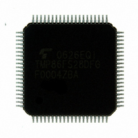
TMP86FS28DFG(JZ) Toshiba, TMP86FS28DFG(JZ) Datasheet - Page 51

TMP86FS28DFG(JZ)
Manufacturer Part Number
TMP86FS28DFG(JZ)
Description
IC MCU 8BIT FLASH 60KB 80-LQFP
Manufacturer
Toshiba
Series
TLCS-870/Cr
Datasheet
1.TMP86FS28DFGJZ.pdf
(272 pages)
Specifications of TMP86FS28DFG(JZ)
Core Processor
870/C
Core Size
8-Bit
Speed
16MHz
Connectivity
SIO, UART/USART
Peripherals
LCD, PWM, WDT
Number Of I /o
62
Program Memory Size
60KB (60K x 8)
Program Memory Type
FLASH
Ram Size
2K x 8
Voltage - Supply (vcc/vdd)
2.7 V ~ 5.5 V
Data Converters
A/D 8x10b
Oscillator Type
Internal
Operating Temperature
-40°C ~ 85°C
Package / Case
80-LQFP
Processor Series
TLCS-870
Core
870/C
Data Bus Width
8 bit
Data Ram Size
2 KB
Interface Type
SIO, UART
Maximum Clock Frequency
16 MHz
Number Of Programmable I/os
62
Number Of Timers
6
Maximum Operating Temperature
+ 85 C
Mounting Style
SMD/SMT
Development Tools By Supplier
BM1040R0A, BMP86A100010A, BMP86A100010B, BMP86A200010B, BMP86A200020A, BMP86A300010A, BMP86A300020A, BMP86A300030A, SW89CN0-ZCC, SW00MN0-ZCC
Minimum Operating Temperature
- 40 C
On-chip Adc
10 bit, 8 Channel
For Use With
BM1401W0A-G - FLASH WRITER ON-BOARD PROGRAMTMP89C900XBG - EMULATION CHIP TMP89F LQFP
Lead Free Status / RoHS Status
Lead free / RoHS Compliant
Eeprom Size
-
Lead Free Status / Rohs Status
Details
Other names
TMP86FS28DFGJZ
Available stocks
Company
Part Number
Manufacturer
Quantity
Price
- Current page: 51 of 272
- Download datasheet (3Mb)
3.3 Interrupt Sequence
Interrupt
request
Interrupt
latch (IL)
IMF
Execute
instruction
PC
SP
3.3.1 Interrupt acceptance processing is packaged as follows.
“0” by resetting or an instruction. Interrupt acceptance sequence requires 8 machine cycles (2 µs @16 MHz) after the
completion of the current instruction. The interrupt service task terminates upon execution of an interrupt return
instruction [RETI] (for maskable interrupts) or [RETN] (for non-maskable interrupts). Figure 3-1 shows the timing
chart of interrupt acceptance processing.
An interrupt request, which raised interrupt latch, is held, until interrupt is accepted or interrupt latch is cleared to
Note 1: a: Return address entry address, b: Entry address, c: Address which RETI instruction is stored
Note 2: On condition that interrupt is enabled, it takes 38/fc [s] or 38/fs [s] at maximum (If the interrupt latch is set at the first
1-machine cycle
Figure 3-1 Timing Chart of Interrupt Acceptance/Return Interrupt Instruction
service program
a − 1
Note:When the contents of PSW are saved on the stack, the contents of IMF are also saved.
Example: Correspondence between vector table address for INTTBT and the entry address of the interrupt
machine cycle on 10 cycle instruction) to start interrupt acceptance processing since its interrupt latch is set.
instruction
a. The interrupt master enable flag (IMF) is cleared to “0” in order to disable the acceptance of any fol-
b. The interrupt latch (IL) for the interrupt source accepted is cleared to “0”.
c. The contents of the program counter (PC) and the program status word, including the interrupt master
d. The entry address (Interrupt vector) of the corresponding interrupt service program, loaded on the vec-
e. The instruction stored at the entry address of the interrupt service program is executed.
Execute
a
lowing interrupt.
enable flag (IMF), are saved (Pushed) on the stack in sequence of PSW + IMF, PCH, PCL. Mean-
while, the stack pointer (SP) is decremented by 3.
tor table, is transferred to the program counter.
a + 1
FFF2H
FFF3H
Vector table address
n
Figure 3-2 Vector table address,Entry address
D2H
03H
Interrupt acceptance
a
n − 1
Vector
n − 2
Page 39
b
b + 1
b + 2
instruction
Execute
b + 3
n - 3
D203H
D204H
Entry address
c + 1
Interrupt service task
0FH
06H
n − 2 n − 1
c + 2
Execute RETI instruction
Interrupt
service
program
TMP86FS28DFG
a
a + 1
n
a + 2
Related parts for TMP86FS28DFG(JZ)
Image
Part Number
Description
Manufacturer
Datasheet
Request
R
Part Number:
Description:
Toshiba Semiconductor [TOSHIBA IGBT Module Silicon N Channel IGBT]
Manufacturer:
TOSHIBA Semiconductor CORPORATION
Datasheet:
Part Number:
Description:
TOSHIBA GTR MODULE SILICON NPN TRIPLE DIFFUSED TYPE
Manufacturer:
TOSHIBA Semiconductor CORPORATION
Datasheet:
Part Number:
Description:
TOSHIBA GTR Module Silicon N Channel IGBT
Manufacturer:
TOSHIBA Semiconductor CORPORATION
Datasheet:
Part Number:
Description:
TOSHIBA Intelligent Power Module Silicon N Channel IGBT
Manufacturer:
TOSHIBA Semiconductor CORPORATION
Datasheet:
Part Number:
Description:
TOSHIBA INTELLIGENT POWER MODULE SILICON N CHANNEL LGBT
Manufacturer:
TOSHIBA Semiconductor CORPORATION
Datasheet:
Part Number:
Description:
TOSHIBA IGBT Module Silicon N Channel IGBT
Manufacturer:
TOSHIBA Semiconductor CORPORATION
Datasheet:
Part Number:
Description:
TOSHIBA GTR MODULE SILICON N−CHANNEL IGBT
Manufacturer:
TOSHIBA Semiconductor CORPORATION
Datasheet:
Part Number:
Description:
TOSHIBA Intelligent Power Module Silicon N Channel IGBT
Manufacturer:
TOSHIBA Semiconductor CORPORATION
Datasheet:
Part Number:
Description:
TOSHIBA GTR Module Silicon N Channel IGBT
Manufacturer:
TOSHIBA Semiconductor CORPORATION
Datasheet:
Part Number:
Description:
TOSHIBA INTELLIGENT POWER MODULE
Manufacturer:
TOSHIBA Semiconductor CORPORATION
Datasheet:
Part Number:
Description:
TOSHIBA Intelligent Power Module Silicon N Channel IGBT
Manufacturer:
TOSHIBA Semiconductor CORPORATION
Datasheet:
Part Number:
Description:
TOSHIBA Intelligent Power Module Silicon N Channel IGBT
Manufacturer:
TOSHIBA Semiconductor CORPORATION
Datasheet:
Part Number:
Description:
TOSHIBA IGBT Module Silicon N Channel IGBT
Manufacturer:
TOSHIBA Semiconductor CORPORATION
Datasheet:
Part Number:
Description:
TOSHIBA Intelligent Power Module Silicon N Channel IGBT
Manufacturer:
TOSHIBA Semiconductor CORPORATION
Datasheet:
Part Number:
Description:
Toshiba Semiconductor [SILICON N CHANNEL 1GBT]
Manufacturer:
TOSHIBA Semiconductor CORPORATION
Datasheet:


