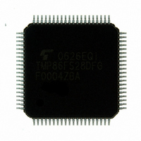
TMP86FS28DFG(JZ) Toshiba, TMP86FS28DFG(JZ) Datasheet - Page 225

TMP86FS28DFG(JZ)
Manufacturer Part Number
TMP86FS28DFG(JZ)
Description
IC MCU 8BIT FLASH 60KB 80-LQFP
Manufacturer
Toshiba
Series
TLCS-870/Cr
Datasheet
1.TMP86FS28DFGJZ.pdf
(272 pages)
Specifications of TMP86FS28DFG(JZ)
Core Processor
870/C
Core Size
8-Bit
Speed
16MHz
Connectivity
SIO, UART/USART
Peripherals
LCD, PWM, WDT
Number Of I /o
62
Program Memory Size
60KB (60K x 8)
Program Memory Type
FLASH
Ram Size
2K x 8
Voltage - Supply (vcc/vdd)
2.7 V ~ 5.5 V
Data Converters
A/D 8x10b
Oscillator Type
Internal
Operating Temperature
-40°C ~ 85°C
Package / Case
80-LQFP
Processor Series
TLCS-870
Core
870/C
Data Bus Width
8 bit
Data Ram Size
2 KB
Interface Type
SIO, UART
Maximum Clock Frequency
16 MHz
Number Of Programmable I/os
62
Number Of Timers
6
Maximum Operating Temperature
+ 85 C
Mounting Style
SMD/SMT
Development Tools By Supplier
BM1040R0A, BMP86A100010A, BMP86A100010B, BMP86A200010B, BMP86A200020A, BMP86A300010A, BMP86A300020A, BMP86A300030A, SW89CN0-ZCC, SW00MN0-ZCC
Minimum Operating Temperature
- 40 C
On-chip Adc
10 bit, 8 Channel
For Use With
BM1401W0A-G - FLASH WRITER ON-BOARD PROGRAMTMP89C900XBG - EMULATION CHIP TMP89F LQFP
Lead Free Status / RoHS Status
Lead free / RoHS Compliant
Eeprom Size
-
Lead Free Status / Rohs Status
Details
Other names
TMP86FS28DFGJZ
Available stocks
Company
Part Number
Manufacturer
Quantity
Price
- Current page: 225 of 272
- Download datasheet (3Mb)
17.2.3 Chip Erase (All Erase)
17.2.4 Product ID Entry
17.2.5 Product ID Exit
17.2.6 Read Protect
Note: The value at address F002H (flash size) depends on the size of flash memory incorporated in each product. For example, if
erase operation is completed. To check the completion of the erase operation, perform read operations repeat-
edly for data polling until the same data is read twice from the same address in the flash memory. During the
erase operation, any consecutive attempts to read from the same address is reversed bit 6 of the data (toggling
between 0 and 1).
be executed until the erase operation is completed. To check the completion of the erase operation, perform
read operations repeatedly for data polling until the same data is read twice from the same address in the flash
memory. During the erase operation, any consecutive attempts to read from the same address is reversed bit 6
of the data (toggling between 0 and 1). After the chip is erased, all bytes contain FFH.
read protection status can be read from the flash memory.
the flash memory cannot be read in the parallel PROM mode. In the serial PROM mode, the flash write com-
mand cannot be executed.
cuting the read protect command sequence. To disable the read protection setting, it is necessary to execute the
chip erase command sequence. Whether or not the read protection is enabled can be checked by reading
FF7FH in the Product ID mode. For details, see Table 17-4.
A maximum of 30 ms is required to erase 4 kbytes. The next command sequence cannot be executed until the
This command erases the entire flash memory in approximately 30 ms. The next command sequence cannot
This command activates the Product ID mode. In the Product ID mode, the vendor ID, the flash ID, and the
the product has 60-kbyte flash memory, "0EH" is read from address F002H.
This command is used to exit the Product ID mode.
This command enables the read protection setting in the flash memory. When the read protection is enabled,
To enable the read protection setting in the serial PROM mode, set FLSCR<BANKSEL> to "1" before exe-
Table 17-4 Values To Be Read in the Product ID Mode
Address
F000H
F001H
F002H
FF7FH
Read protection status
Flash macro ID
Vendor ID
Flash size
Meaning
Page 213
98H
41H
0EH:
0BH:
07H:
05H:
03H:
01H:
00H:
FFH:
Other than FFH: Read protection enabled
60 kbytes
48 kbytes
32 kbytes
24 kbytes
16 kbytes
8 kbytes
4 kbytes
Read protection disabled
Read Value
TMP86FS28DFG
Related parts for TMP86FS28DFG(JZ)
Image
Part Number
Description
Manufacturer
Datasheet
Request
R
Part Number:
Description:
Toshiba Semiconductor [TOSHIBA IGBT Module Silicon N Channel IGBT]
Manufacturer:
TOSHIBA Semiconductor CORPORATION
Datasheet:
Part Number:
Description:
TOSHIBA GTR MODULE SILICON NPN TRIPLE DIFFUSED TYPE
Manufacturer:
TOSHIBA Semiconductor CORPORATION
Datasheet:
Part Number:
Description:
TOSHIBA GTR Module Silicon N Channel IGBT
Manufacturer:
TOSHIBA Semiconductor CORPORATION
Datasheet:
Part Number:
Description:
TOSHIBA Intelligent Power Module Silicon N Channel IGBT
Manufacturer:
TOSHIBA Semiconductor CORPORATION
Datasheet:
Part Number:
Description:
TOSHIBA INTELLIGENT POWER MODULE SILICON N CHANNEL LGBT
Manufacturer:
TOSHIBA Semiconductor CORPORATION
Datasheet:
Part Number:
Description:
TOSHIBA IGBT Module Silicon N Channel IGBT
Manufacturer:
TOSHIBA Semiconductor CORPORATION
Datasheet:
Part Number:
Description:
TOSHIBA GTR MODULE SILICON N−CHANNEL IGBT
Manufacturer:
TOSHIBA Semiconductor CORPORATION
Datasheet:
Part Number:
Description:
TOSHIBA Intelligent Power Module Silicon N Channel IGBT
Manufacturer:
TOSHIBA Semiconductor CORPORATION
Datasheet:
Part Number:
Description:
TOSHIBA GTR Module Silicon N Channel IGBT
Manufacturer:
TOSHIBA Semiconductor CORPORATION
Datasheet:
Part Number:
Description:
TOSHIBA INTELLIGENT POWER MODULE
Manufacturer:
TOSHIBA Semiconductor CORPORATION
Datasheet:
Part Number:
Description:
TOSHIBA Intelligent Power Module Silicon N Channel IGBT
Manufacturer:
TOSHIBA Semiconductor CORPORATION
Datasheet:
Part Number:
Description:
TOSHIBA Intelligent Power Module Silicon N Channel IGBT
Manufacturer:
TOSHIBA Semiconductor CORPORATION
Datasheet:
Part Number:
Description:
TOSHIBA IGBT Module Silicon N Channel IGBT
Manufacturer:
TOSHIBA Semiconductor CORPORATION
Datasheet:
Part Number:
Description:
TOSHIBA Intelligent Power Module Silicon N Channel IGBT
Manufacturer:
TOSHIBA Semiconductor CORPORATION
Datasheet:
Part Number:
Description:
Toshiba Semiconductor [SILICON N CHANNEL 1GBT]
Manufacturer:
TOSHIBA Semiconductor CORPORATION
Datasheet:


