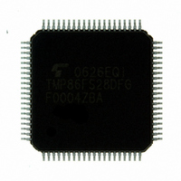
TMP86FS28DFG(JZ) Toshiba, TMP86FS28DFG(JZ) Datasheet - Page 201

TMP86FS28DFG(JZ)
Manufacturer Part Number
TMP86FS28DFG(JZ)
Description
IC MCU 8BIT FLASH 60KB 80-LQFP
Manufacturer
Toshiba
Series
TLCS-870/Cr
Datasheet
1.TMP86FS28DFGJZ.pdf
(272 pages)
Specifications of TMP86FS28DFG(JZ)
Core Processor
870/C
Core Size
8-Bit
Speed
16MHz
Connectivity
SIO, UART/USART
Peripherals
LCD, PWM, WDT
Number Of I /o
62
Program Memory Size
60KB (60K x 8)
Program Memory Type
FLASH
Ram Size
2K x 8
Voltage - Supply (vcc/vdd)
2.7 V ~ 5.5 V
Data Converters
A/D 8x10b
Oscillator Type
Internal
Operating Temperature
-40°C ~ 85°C
Package / Case
80-LQFP
Processor Series
TLCS-870
Core
870/C
Data Bus Width
8 bit
Data Ram Size
2 KB
Interface Type
SIO, UART
Maximum Clock Frequency
16 MHz
Number Of Programmable I/os
62
Number Of Timers
6
Maximum Operating Temperature
+ 85 C
Mounting Style
SMD/SMT
Development Tools By Supplier
BM1040R0A, BMP86A100010A, BMP86A100010B, BMP86A200010B, BMP86A200020A, BMP86A300010A, BMP86A300020A, BMP86A300030A, SW89CN0-ZCC, SW00MN0-ZCC
Minimum Operating Temperature
- 40 C
On-chip Adc
10 bit, 8 Channel
For Use With
BM1401W0A-G - FLASH WRITER ON-BOARD PROGRAMTMP89C900XBG - EMULATION CHIP TMP89F LQFP
Lead Free Status / RoHS Status
Lead free / RoHS Compliant
Eeprom Size
-
Lead Free Status / Rohs Status
Details
Other names
TMP86FS28DFGJZ
Available stocks
Company
Part Number
Manufacturer
Quantity
Price
- Current page: 201 of 272
- Download datasheet (3Mb)
14.6 Precautions about AD Converter
14.6.1 Analog input pin voltage range
14.6.2 Analog input shared pins
14.6.3 Noise Countermeasure
Figure 14-5
Permissible signal
source impedance
5 kΩ (max)
outside this range is applied to one of the analog input pins, the converted value on that pin becomes uncertain.
The other analog input pins also are affected by that.
inputs to execute AD conversion, do not execute input/output instructions for all other ports. This is necessary
to prevent the accuracy of AD conversion from degrading. Not only these analog input shared pins, some other
pins may also be affected by noise arising from input/output to and from adjacent pins.
impedance of the analog input source, more easily they are susceptible to noise. Therefore, make sure the out-
put impedance of the signal source in your design is 5 kΩ or less. Toshiba also recommends attaching a capac-
itor external to the chip.
Make sure the analog input pins (AIN0 to AIN7) are used at voltages within VAREF to AVSS. If any voltage
The analog input pins (AIN0 to AIN7) are shared with input/output ports. When using any of the analog
The internal equivalent circuit of the analog input pins is shown in Figure 14-5. The higher the output
Note) i = 7 to 0
Analog Input Equivalent Circuit and Example of Input Pin Processing
AINi
Internal resistance
5 kΩ (typ)
Internal capacitance
Page 189
C = 22 pF (typ.)
Analog comparator
DA converter
TMP86FS28DFG
Related parts for TMP86FS28DFG(JZ)
Image
Part Number
Description
Manufacturer
Datasheet
Request
R
Part Number:
Description:
Toshiba Semiconductor [TOSHIBA IGBT Module Silicon N Channel IGBT]
Manufacturer:
TOSHIBA Semiconductor CORPORATION
Datasheet:
Part Number:
Description:
TOSHIBA GTR MODULE SILICON NPN TRIPLE DIFFUSED TYPE
Manufacturer:
TOSHIBA Semiconductor CORPORATION
Datasheet:
Part Number:
Description:
TOSHIBA GTR Module Silicon N Channel IGBT
Manufacturer:
TOSHIBA Semiconductor CORPORATION
Datasheet:
Part Number:
Description:
TOSHIBA Intelligent Power Module Silicon N Channel IGBT
Manufacturer:
TOSHIBA Semiconductor CORPORATION
Datasheet:
Part Number:
Description:
TOSHIBA INTELLIGENT POWER MODULE SILICON N CHANNEL LGBT
Manufacturer:
TOSHIBA Semiconductor CORPORATION
Datasheet:
Part Number:
Description:
TOSHIBA IGBT Module Silicon N Channel IGBT
Manufacturer:
TOSHIBA Semiconductor CORPORATION
Datasheet:
Part Number:
Description:
TOSHIBA GTR MODULE SILICON N−CHANNEL IGBT
Manufacturer:
TOSHIBA Semiconductor CORPORATION
Datasheet:
Part Number:
Description:
TOSHIBA Intelligent Power Module Silicon N Channel IGBT
Manufacturer:
TOSHIBA Semiconductor CORPORATION
Datasheet:
Part Number:
Description:
TOSHIBA GTR Module Silicon N Channel IGBT
Manufacturer:
TOSHIBA Semiconductor CORPORATION
Datasheet:
Part Number:
Description:
TOSHIBA INTELLIGENT POWER MODULE
Manufacturer:
TOSHIBA Semiconductor CORPORATION
Datasheet:
Part Number:
Description:
TOSHIBA Intelligent Power Module Silicon N Channel IGBT
Manufacturer:
TOSHIBA Semiconductor CORPORATION
Datasheet:
Part Number:
Description:
TOSHIBA Intelligent Power Module Silicon N Channel IGBT
Manufacturer:
TOSHIBA Semiconductor CORPORATION
Datasheet:
Part Number:
Description:
TOSHIBA IGBT Module Silicon N Channel IGBT
Manufacturer:
TOSHIBA Semiconductor CORPORATION
Datasheet:
Part Number:
Description:
TOSHIBA Intelligent Power Module Silicon N Channel IGBT
Manufacturer:
TOSHIBA Semiconductor CORPORATION
Datasheet:
Part Number:
Description:
Toshiba Semiconductor [SILICON N CHANNEL 1GBT]
Manufacturer:
TOSHIBA Semiconductor CORPORATION
Datasheet:


