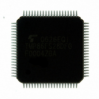
TMP86FS28DFG(JZ) Toshiba, TMP86FS28DFG(JZ) Datasheet - Page 178

TMP86FS28DFG(JZ)
Manufacturer Part Number
TMP86FS28DFG(JZ)
Description
IC MCU 8BIT FLASH 60KB 80-LQFP
Manufacturer
Toshiba
Series
TLCS-870/Cr
Datasheet
1.TMP86FS28DFGJZ.pdf
(272 pages)
Specifications of TMP86FS28DFG(JZ)
Core Processor
870/C
Core Size
8-Bit
Speed
16MHz
Connectivity
SIO, UART/USART
Peripherals
LCD, PWM, WDT
Number Of I /o
62
Program Memory Size
60KB (60K x 8)
Program Memory Type
FLASH
Ram Size
2K x 8
Voltage - Supply (vcc/vdd)
2.7 V ~ 5.5 V
Data Converters
A/D 8x10b
Oscillator Type
Internal
Operating Temperature
-40°C ~ 85°C
Package / Case
80-LQFP
Processor Series
TLCS-870
Core
870/C
Data Bus Width
8 bit
Data Ram Size
2 KB
Interface Type
SIO, UART
Maximum Clock Frequency
16 MHz
Number Of Programmable I/os
62
Number Of Timers
6
Maximum Operating Temperature
+ 85 C
Mounting Style
SMD/SMT
Development Tools By Supplier
BM1040R0A, BMP86A100010A, BMP86A100010B, BMP86A200010B, BMP86A200020A, BMP86A300010A, BMP86A300020A, BMP86A300030A, SW89CN0-ZCC, SW00MN0-ZCC
Minimum Operating Temperature
- 40 C
On-chip Adc
10 bit, 8 Channel
For Use With
BM1401W0A-G - FLASH WRITER ON-BOARD PROGRAMTMP89C900XBG - EMULATION CHIP TMP89F LQFP
Lead Free Status / RoHS Status
Lead free / RoHS Compliant
Eeprom Size
-
Lead Free Status / Rohs Status
Details
Other names
TMP86FS28DFGJZ
Available stocks
Company
Part Number
Manufacturer
Quantity
Price
- Current page: 178 of 272
- Download datasheet (3Mb)
12.6 STOP Bit Length
12.6 STOP Bit Length
12.7 Parity
12.8 Transmit/Receive Operation
12.8.1 Data Transmit Operation
12.8.2 Data Receive Operation
UART1CR1<EVEN>.
Select a transmit stop bit length (1 bit or 2 bits) by UART1CR1<STBT>.
Set parity / no parity by UART1CR1<PE> and set parity type (Odd- or Even-numbered) by
TD1BUF (Transmit data buffer). Writing data in TD1BUF zero-clears UART1SR<TBEP>, transfers the data
to the transmit shift register and the data are sequentially output from the TXD1 pin. The data output include a
one-bit start bit, stop bits whose number is specified in UART1CR1<STBT> and a parity bit if parity addition
is specified. Select the data transfer baud rate using UART1CR1<BRG>. When data transmit starts, transmit
buffer empty flag UART1SR<TBEP> is set to “1” and an INTTXD1 interrupt is generated.
written to TD1BUF, the TXD1 pin is fixed at high level.
When transmitting data, first read UART1SR, then write data in TD1BUF. Otherwise, UART1SR<TBEP> is
not zero-cleared and transmit does not start.
RD1BUF (Receive data buffer). At this time, the data transmitted includes a start bit and stop bit(s) and a parity
bit if parity addition is specified. When stop bit(s) are received, data only are extracted and transferred to
RD1BUF (Receive data buffer). Then the receive buffer full flag UART1SR<RBFL> is set and an INTRXD1
interrupt is generated. Select the data transfer baud rate using UART1CR1<BRG>.
data buffer) but discarded; data in the RD1BUF are not affected.
Set UART1CR1<TXE> to “1”. Read UART1SR to check UART1SR<TBEP> = “1”, then write data in
While UART1CR1<TXE> = “0” and from when “1” is written to UART1CR1<TXE> to when send data are
Set UART1CR1<RXE> to “1”. When data are received via the RXD1 pin, the receive data are transferred to
If an overrun error (OERR) occurs when data are received, the data are not transferred to RD1BUF (Receive
Note:When a receive operation is disabled by setting UART1CR1<RXE> bit to “0”, the setting becomes valid when
data receive is completed. However, if a framing error occurs in data receive, the receive-disabling setting
may not become valid. If a framing error occurs, be sure to perform a re-receive operation.
Page 166
TMP86FS28DFG
Related parts for TMP86FS28DFG(JZ)
Image
Part Number
Description
Manufacturer
Datasheet
Request
R
Part Number:
Description:
Toshiba Semiconductor [TOSHIBA IGBT Module Silicon N Channel IGBT]
Manufacturer:
TOSHIBA Semiconductor CORPORATION
Datasheet:
Part Number:
Description:
TOSHIBA GTR MODULE SILICON NPN TRIPLE DIFFUSED TYPE
Manufacturer:
TOSHIBA Semiconductor CORPORATION
Datasheet:
Part Number:
Description:
TOSHIBA GTR Module Silicon N Channel IGBT
Manufacturer:
TOSHIBA Semiconductor CORPORATION
Datasheet:
Part Number:
Description:
TOSHIBA Intelligent Power Module Silicon N Channel IGBT
Manufacturer:
TOSHIBA Semiconductor CORPORATION
Datasheet:
Part Number:
Description:
TOSHIBA INTELLIGENT POWER MODULE SILICON N CHANNEL LGBT
Manufacturer:
TOSHIBA Semiconductor CORPORATION
Datasheet:
Part Number:
Description:
TOSHIBA IGBT Module Silicon N Channel IGBT
Manufacturer:
TOSHIBA Semiconductor CORPORATION
Datasheet:
Part Number:
Description:
TOSHIBA GTR MODULE SILICON N−CHANNEL IGBT
Manufacturer:
TOSHIBA Semiconductor CORPORATION
Datasheet:
Part Number:
Description:
TOSHIBA Intelligent Power Module Silicon N Channel IGBT
Manufacturer:
TOSHIBA Semiconductor CORPORATION
Datasheet:
Part Number:
Description:
TOSHIBA GTR Module Silicon N Channel IGBT
Manufacturer:
TOSHIBA Semiconductor CORPORATION
Datasheet:
Part Number:
Description:
TOSHIBA INTELLIGENT POWER MODULE
Manufacturer:
TOSHIBA Semiconductor CORPORATION
Datasheet:
Part Number:
Description:
TOSHIBA Intelligent Power Module Silicon N Channel IGBT
Manufacturer:
TOSHIBA Semiconductor CORPORATION
Datasheet:
Part Number:
Description:
TOSHIBA Intelligent Power Module Silicon N Channel IGBT
Manufacturer:
TOSHIBA Semiconductor CORPORATION
Datasheet:
Part Number:
Description:
TOSHIBA IGBT Module Silicon N Channel IGBT
Manufacturer:
TOSHIBA Semiconductor CORPORATION
Datasheet:
Part Number:
Description:
TOSHIBA Intelligent Power Module Silicon N Channel IGBT
Manufacturer:
TOSHIBA Semiconductor CORPORATION
Datasheet:
Part Number:
Description:
Toshiba Semiconductor [SILICON N CHANNEL 1GBT]
Manufacturer:
TOSHIBA Semiconductor CORPORATION
Datasheet:


