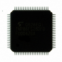
TMP86FS28DFG(JZ) Toshiba, TMP86FS28DFG(JZ) Datasheet - Page 164

TMP86FS28DFG(JZ)
Manufacturer Part Number
TMP86FS28DFG(JZ)
Description
IC MCU 8BIT FLASH 60KB 80-LQFP
Manufacturer
Toshiba
Series
TLCS-870/Cr
Datasheet
1.TMP86FS28DFGJZ.pdf
(272 pages)
Specifications of TMP86FS28DFG(JZ)
Core Processor
870/C
Core Size
8-Bit
Speed
16MHz
Connectivity
SIO, UART/USART
Peripherals
LCD, PWM, WDT
Number Of I /o
62
Program Memory Size
60KB (60K x 8)
Program Memory Type
FLASH
Ram Size
2K x 8
Voltage - Supply (vcc/vdd)
2.7 V ~ 5.5 V
Data Converters
A/D 8x10b
Oscillator Type
Internal
Operating Temperature
-40°C ~ 85°C
Package / Case
80-LQFP
Processor Series
TLCS-870
Core
870/C
Data Bus Width
8 bit
Data Ram Size
2 KB
Interface Type
SIO, UART
Maximum Clock Frequency
16 MHz
Number Of Programmable I/os
62
Number Of Timers
6
Maximum Operating Temperature
+ 85 C
Mounting Style
SMD/SMT
Development Tools By Supplier
BM1040R0A, BMP86A100010A, BMP86A100010B, BMP86A200010B, BMP86A200020A, BMP86A300010A, BMP86A300020A, BMP86A300030A, SW89CN0-ZCC, SW00MN0-ZCC
Minimum Operating Temperature
- 40 C
On-chip Adc
10 bit, 8 Channel
For Use With
BM1401W0A-G - FLASH WRITER ON-BOARD PROGRAMTMP89C900XBG - EMULATION CHIP TMP89F LQFP
Lead Free Status / RoHS Status
Lead free / RoHS Compliant
Eeprom Size
-
Lead Free Status / Rohs Status
Details
Other names
TMP86FS28DFGJZ
Available stocks
Company
Part Number
Manufacturer
Quantity
Price
- Current page: 164 of 272
- Download datasheet (3Mb)
11.2 Control
11.2 Control
SIO Control Register 2
SIO Control Register 1
determined by reading SIO status register (SIOSR).
0F60H to 0F67H for SIO in the DBR area, and can continuously transfer up to 8 words (bytes or nibbles) at one time.
When the specified number of words has been transferred, a buffer empty (in the transmit mode) or a buffer full (in
the receive mode or transmit/receive mode) interrupt (INTSIO) is generated.
fixed interval wait can be applied to the serial clock for each word transferred. Four different wait times can be
selected with SIOCR2<WAIT>.
The serial interface is controlled by SIO control registers (SIOCR1/SIOCR2). The serial interface status can be
The transmit and receive data buffer is controlled by the SIOCR2<BUF>. The data buffer is assigned to address
When the internal clock is used as the serial clock in the 8-bit receive mode and the 8-bit transmit/receive mode, a
Note 1: fc; High-frequency clock [Hz], fs; Low-frequency clock [Hz]
Note 2: Set SIOS to "0" and SIOINH to "1" when setting the transfer mode or serial clock.
Note 3: SIOCR1 is write-only register, which cannot access any of in read-modify-write instruction such as bit operate, etc.
SIOCR1
(0F68H)
SIOCR2
(0F69H)
SIOINH
SIOM
SIOS
SCK
SIOS
7
7
Indicate transfer start / stop
Continue / abort transfer
Transfer mode select
Serial clock select
SIOINH
6
6
5
5
SIOM
4
4
0:
1:
0:
1:
000:
010:
100:
101:
110:
Except the above: Reserved
WAIT
000
001
010
011
100
101
110
111
Page 152
3
Stop
Start
Continuously transfer
Abort transfer (Automatically cleared after abort)
8-bit transmit mode
4-bit transmit mode
8-bit transmit / receive mode
8-bit receive mode
4-bit receive mode
3
DV7CK = 0
2
2
NORMAL1/2, IDLE1/2 mode
fc/2
fc/2
fc/2
fc/2
fc/2
fc/2
13
8
7
6
5
4
External clock ( Input from SCK pin )
SCK
BUF
1
1
DV7CK = 1
Reserved
0
0
fs/2
fc/2
fc/2
fc/2
fc/2
fc/2
5
8
7
6
5
4
(Initial value: 0000 0000)
(Initial value: ***0 0000)
SLEEP1/2
SLOW1/2
TMP86FS28DFG
mode
fs/2
-
-
-
-
-
5
Write
Write
only
only
Related parts for TMP86FS28DFG(JZ)
Image
Part Number
Description
Manufacturer
Datasheet
Request
R
Part Number:
Description:
Toshiba Semiconductor [TOSHIBA IGBT Module Silicon N Channel IGBT]
Manufacturer:
TOSHIBA Semiconductor CORPORATION
Datasheet:
Part Number:
Description:
TOSHIBA GTR MODULE SILICON NPN TRIPLE DIFFUSED TYPE
Manufacturer:
TOSHIBA Semiconductor CORPORATION
Datasheet:
Part Number:
Description:
TOSHIBA GTR Module Silicon N Channel IGBT
Manufacturer:
TOSHIBA Semiconductor CORPORATION
Datasheet:
Part Number:
Description:
TOSHIBA Intelligent Power Module Silicon N Channel IGBT
Manufacturer:
TOSHIBA Semiconductor CORPORATION
Datasheet:
Part Number:
Description:
TOSHIBA INTELLIGENT POWER MODULE SILICON N CHANNEL LGBT
Manufacturer:
TOSHIBA Semiconductor CORPORATION
Datasheet:
Part Number:
Description:
TOSHIBA IGBT Module Silicon N Channel IGBT
Manufacturer:
TOSHIBA Semiconductor CORPORATION
Datasheet:
Part Number:
Description:
TOSHIBA GTR MODULE SILICON N−CHANNEL IGBT
Manufacturer:
TOSHIBA Semiconductor CORPORATION
Datasheet:
Part Number:
Description:
TOSHIBA Intelligent Power Module Silicon N Channel IGBT
Manufacturer:
TOSHIBA Semiconductor CORPORATION
Datasheet:
Part Number:
Description:
TOSHIBA GTR Module Silicon N Channel IGBT
Manufacturer:
TOSHIBA Semiconductor CORPORATION
Datasheet:
Part Number:
Description:
TOSHIBA INTELLIGENT POWER MODULE
Manufacturer:
TOSHIBA Semiconductor CORPORATION
Datasheet:
Part Number:
Description:
TOSHIBA Intelligent Power Module Silicon N Channel IGBT
Manufacturer:
TOSHIBA Semiconductor CORPORATION
Datasheet:
Part Number:
Description:
TOSHIBA Intelligent Power Module Silicon N Channel IGBT
Manufacturer:
TOSHIBA Semiconductor CORPORATION
Datasheet:
Part Number:
Description:
TOSHIBA IGBT Module Silicon N Channel IGBT
Manufacturer:
TOSHIBA Semiconductor CORPORATION
Datasheet:
Part Number:
Description:
TOSHIBA Intelligent Power Module Silicon N Channel IGBT
Manufacturer:
TOSHIBA Semiconductor CORPORATION
Datasheet:
Part Number:
Description:
Toshiba Semiconductor [SILICON N CHANNEL 1GBT]
Manufacturer:
TOSHIBA Semiconductor CORPORATION
Datasheet:


