PXAS30KFA,512 NXP Semiconductors, PXAS30KFA,512 Datasheet - Page 15
PXAS30KFA,512
Manufacturer Part Number
PXAS30KFA,512
Description
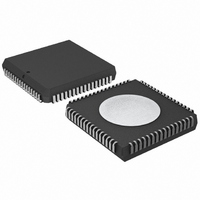
IC XA MCU 16BIT ROMLESS 68-PLCC
Manufacturer
NXP Semiconductors
Series
XAr
Datasheet
1.PXAS30KBA512.pdf
(52 pages)
Specifications of PXAS30KFA,512
Core Processor
XA
Core Size
16-Bit
Speed
30MHz
Connectivity
EBI/EMI, I²C, UART/USART
Peripherals
PWM, WDT
Number Of I /o
32
Program Memory Type
ROMless
Ram Size
1K x 8
Voltage - Supply (vcc/vdd)
2.7 V ~ 5.5 V
Data Converters
A/D 8x8b
Oscillator Type
External
Operating Temperature
-40°C ~ 85°C
Package / Case
68-PLCC
Processor Series
PXAS3x
Core
80C51
Data Bus Width
16 bit
Data Ram Size
1 KB
Interface Type
I2C, UART
Maximum Clock Frequency
30 MHz
Number Of Programmable I/os
50
Number Of Timers
3
Operating Supply Voltage
2.7 V to 5.5 V
Maximum Operating Temperature
+ 85 C
Mounting Style
SMD/SMT
Minimum Operating Temperature
- 40 C
On-chip Adc
8 bit, 8 Channel
Lead Free Status / RoHS Status
Lead free / RoHS Compliant
Eeprom Size
-
Program Memory Size
-
Lead Free Status / Rohs Status
Details
Other names
568-3535-5
935262382512
PXAS30KFA
935262382512
PXAS30KFA
Available stocks
Company
Part Number
Manufacturer
Quantity
Price
Company:

Part Number:
PXAS30KFA,512
Manufacturer:
NXP Semiconductors
Quantity:
10 000


1. These settings provide additional A/D input sampling time, in order to allow accurate readings with a higher external source impedance.
Philips Semiconductors
Table 2. A/D Timing Configuration
NOTE:
2000 Dec 01
0h (0000)
1h (0001)
2h (0010)
3h (0011)
4h (0100)
5h (0101)
6h (0110)
7h (0111)
8h (1000)
9h (1001)
Ah (1010)
Bh (1011)
Ch (1100)
Dh (1101)
Eh (1110)
Fh (1111)
XA 16-bit microcontroller
32 K/1 K OTP/ROM/ROMless, 8-channel 8-bit A/D, low voltage (2.7 V–5.5 V),
I
ADCS
Bit Addressable
Reset Value: 00h
ADCFG
Not bit Addressable
Reset Value: 00h
2
C, 2 UARTs, 16 MB address range
ADCFG 3 0
ADCFG.3–0
BIT
ADCS.7
ADCS.6
ADCS.5
ADCS.4
ADCS.3
ADCS.2
ADCS.1
ADCS.0
BIT
ADCFG.7
ADCFG.6
ADCFG.5
ADCFG.4
ADCFG.3–0
1
1
Address:43Fh
Address:4B9h
SYMBOL
ADCS7
ADCS6
ADCS5
ADCS4
ADCS3
ADCS2
ADCS1
ADCS0
SYMBOL
—
—
—
—
ADCFG
Frequency (MHz)
Max. Oscillator
13.33
16.66
11.11
6.66
22.2
23.3
26.6
10
20
20
30
30
–
–
–
–
FUNCTION
A/D channel 7 select bit.
A/D channel 6 select bit.
A/D channel 5 select bit.
A/D channel 4 select bit.
A/D channel 3 select bit.
A/D channel 2 select bit.
A/D channel 1 select bit.
A/D channel 0 select bit.
FUNCTION
Reserved for future use. Should not be set to 1 by user programs.
Reserved for future use. Should not be set to 1 by user programs.
Reserved for future use. Should not be set to 1 by user programs.
Reserved for future use. Should not be set to 1 by user programs.
A/D timing configuration (see text and table).
MSB
MSB
ADCS7
Figure 3. A/D Timing Configuration Register (ADCFG)
—
Figure 2. A/D Channel Select Register (ADCS)
ADCS6
—
Osc. Clocks
ADCS5
—
100
104
116
108
124
128
132
146
136
152
172
176
72
76
80
96
15
ADCS4
—
Conversion Time
ADCS3
A/D Timing Configuration
sec at max. Osc.
ADCS2
10.81
4.86
5.32
4.81
4.87
4.25
4.56
7.6
7.2
7.2
6.0
5.2
5.8
4.4
4.7
4.4
ADCS1
ADCS0
SU00940
SU00939
LSB
LSB
Preliminary specification
Sampling Time
(Osc. Clocks)
p
10
12
24
14
14
16
18
32
20
20
22
24
4
6
8
8
g
XA-S3
Related parts for PXAS30KFA,512
Image
Part Number
Description
Manufacturer
Datasheet
Request
R

Part Number:
Description:
NXP Semiconductors designed the LPC2420/2460 microcontroller around a 16-bit/32-bitARM7TDMI-S CPU core with real-time debug interfaces that include both JTAG andembedded trace
Manufacturer:
NXP Semiconductors
Datasheet:

Part Number:
Description:
NXP Semiconductors designed the LPC2458 microcontroller around a 16-bit/32-bitARM7TDMI-S CPU core with real-time debug interfaces that include both JTAG andembedded trace
Manufacturer:
NXP Semiconductors
Datasheet:
Part Number:
Description:
NXP Semiconductors designed the LPC2468 microcontroller around a 16-bit/32-bitARM7TDMI-S CPU core with real-time debug interfaces that include both JTAG andembedded trace
Manufacturer:
NXP Semiconductors
Datasheet:
Part Number:
Description:
NXP Semiconductors designed the LPC2470 microcontroller, powered by theARM7TDMI-S core, to be a highly integrated microcontroller for a wide range ofapplications that require advanced communications and high quality graphic displays
Manufacturer:
NXP Semiconductors
Datasheet:
Part Number:
Description:
NXP Semiconductors designed the LPC2478 microcontroller, powered by theARM7TDMI-S core, to be a highly integrated microcontroller for a wide range ofapplications that require advanced communications and high quality graphic displays
Manufacturer:
NXP Semiconductors
Datasheet:
Part Number:
Description:
The Philips Semiconductors XA (eXtended Architecture) family of 16-bit single-chip microcontrollers is powerful enough to easily handle the requirements of high performance embedded applications, yet inexpensive enough to compete in the market for hi
Manufacturer:
NXP Semiconductors
Datasheet:
Part Number:
Description:
The XA-S3 device is a member of Philips Semiconductors? XA(eXtended Architecture) family of high performance 16-bitsingle-chip microcontrollers
Manufacturer:
NXP Semiconductors
Datasheet:

Part Number:
Description:
The NXP BlueStreak LH75401/LH75411 family consists of two low-cost 16/32-bit System-on-Chip (SoC) devices
Manufacturer:
NXP Semiconductors
Datasheet:
Part Number:
Description:
The NXP LPC3130/3131 combine an 180 MHz ARM926EJ-S CPU core, high-speed USB2
Manufacturer:
NXP Semiconductors
Datasheet:
Part Number:
Description:
The NXP LPC3141 combine a 270 MHz ARM926EJ-S CPU core, High-speed USB 2
Manufacturer:
NXP Semiconductors
Part Number:
Description:
The NXP LPC3143 combine a 270 MHz ARM926EJ-S CPU core, High-speed USB 2
Manufacturer:
NXP Semiconductors

Part Number:
Description:
The NXP LPC3152 combines an 180 MHz ARM926EJ-S CPU core, High-speed USB 2
Manufacturer:
NXP Semiconductors
Part Number:
Description:
The NXP LPC3154 combines an 180 MHz ARM926EJ-S CPU core, High-speed USB 2
Manufacturer:
NXP Semiconductors

Part Number:
Description:
Standard level N-channel enhancement mode Field-Effect Transistor (FET) in a plastic package using NXP High-Performance Automotive (HPA) TrenchMOS technology
Manufacturer:
NXP Semiconductors
Datasheet: