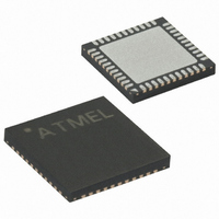
ATMEGA1284P-MUR Atmel, ATMEGA1284P-MUR Datasheet - Page 68

ATMEGA1284P-MUR
Manufacturer Part Number
ATMEGA1284P-MUR
Description
MCU AVR 128KB FLASH 20MHZ 44VQFN
Manufacturer
Atmel
Series
AVR® ATmegar
Specifications of ATMEGA1284P-MUR
Core Processor
AVR
Core Size
8-Bit
Speed
20MHz
Connectivity
I²C, SPI, UART/USART
Peripherals
Brown-out Detect/Reset, POR, PWM, WDT
Number Of I /o
32
Program Memory Size
128KB (64K x 16)
Program Memory Type
FLASH
Eeprom Size
4K x 8
Ram Size
16K x 8
Voltage - Supply (vcc/vdd)
1.8 V ~ 5.5 V
Data Converters
A/D 8x10b
Oscillator Type
Internal
Operating Temperature
-40°C ~ 85°C
Package / Case
44-VQFN Exposed Pad
For Use With
ATSTK600 - DEV KIT FOR AVR/AVR32
Lead Free Status / RoHS Status
Lead free / RoHS Compliant
Available stocks
Company
Part Number
Manufacturer
Quantity
Price
Company:
Part Number:
ATMEGA1284P-MUR
Manufacturer:
FREESCALE
Quantity:
593
- Current page: 68 of 581
- Download datasheet (27Mb)
12. External Interrupts
12.1
12.2
12.2.1
8272A–AVR–01/10
Overview
Register Description
EICRA – External Interrupt Control Register A
The External Interrupts are triggered by the INT2:0 pin or any of the PCINT31:0 pins. Observe
that, if enabled, the interrupts will trigger even if the INT2:0 or PCINT31:0 pins are configured as
outputs. This feature provides a way of generating a software interrupt.
The Pin change interrupt PCI3 will trigger if any enabled PCINT31:24 pin toggle, Pin change
interrupt PCI2 will trigger if any enabled PCINT23:16 pin toggles, Pin change interrupt PCI1 if
any enabled PCINT15:8 toggles and Pin change interrupts PCI0 will trigger if any enabled
PCINT7:0 pin toggles. PCMSK3, PCMSK2, PCMSK1 and PCMSK0 Registers control which pins
contribute to the pin change interrupts. Pin change interrupts on PCINT31:0 are detected asyn-
chronously. This implies that these interrupts can be used for waking the part also from sleep
modes other than Idle mode.
The External Interrupts can be triggered by a falling or rising edge or a low level. This is set up
as indicated in the specification for the External Interrupt Control Registers – EICRA (INT2:0).
When the external interrupt is enabled and is configured as level triggered, the interrupt will trig-
ger as long as the pin is held low. Low level interrupts and the edge interrupt on INT2:0 are
detected asynchronously. This implies that these interrupts can be used for waking the part also
from sleep modes other than Idle mode. The I/O clock is halted in all sleep modes except Idle
mode.
Note that if a level triggered interrupt is used for wake-up from Power-down, the required level
must be held long enough for the MCU to complete the wake-up to trigger the level interrupt. If
the level disappears before the end of the Start-up Time, the MCU will still wake up, but no inter-
rupt will be generated. The start-up time is defined by the SUT and CKSEL Fuses as described
in
The External Interrupt Control Register A contains control bits for interrupt sense control.
• Bits 7:6 – Reserved
These bits are reserved in the ATmega164A/164PA/324A/324PA/644A/644PA/1284/1284P,
and will always read as zero.
• Bits 5:0 – ISC21, ISC20 – ISC00, ISC00: External Interrupt 2 - 0 Sense Control Bits
The External Interrupts 2 - 0 are activated by the external pins INT2:0 if the SREG I-flag and the
corresponding interrupt mask in the EIMSK is set. The level and edges on the external pins that
activate the interrupts are defined in
nously. Pulses on INT2:0 pins wider than the minimum pulse width given in
Characteristics” on page 335
164A/164PA/324A/324PA/644A/644PA/1284/1284P
Bit
(0x69)
Read/Write
Initial Value
”System Clock and Clock Options” on page
R
7
–
0
R
6
–
0
will generate an interrupt. Shorter pulses are not guaranteed to
ISC21
R/W
5
0
Table
ISC20
12-1. Edges on INT2..INT0 are registered asynchro-
R/W
4
0
30.
ISC11
R/W
3
0
ISC10
R/W
2
0
ISC01
R/W
1
0
”External Interrupts
ISC00
R/W
0
0
EICRA
68
Related parts for ATMEGA1284P-MUR
Image
Part Number
Description
Manufacturer
Datasheet
Request
R

Part Number:
Description:
Manufacturer:
ATMEL Corporation
Datasheet:

Part Number:
Description:
Microcontroller with 128K bytes In-system programmable flash, 8 MHz, power supply =2.7 - 5.5V
Manufacturer:
ATMEL Corporation
Datasheet:

Part Number:
Description:
IC AVR MCU 128K 16MHZ 5V 64TQFP
Manufacturer:
Atmel
Datasheet:

Part Number:
Description:
IC AVR MCU 128K 16MHZ 5V 64-QFN
Manufacturer:
Atmel
Datasheet:

Part Number:
Description:
IC AVR MCU 128K 16MHZ COM 64-QFN
Manufacturer:
Atmel
Datasheet:

Part Number:
Description:
IC AVR MCU 128K 16MHZ 64-TQFP
Manufacturer:
Atmel
Datasheet:

Part Number:
Description:
IC AVR MCU 128K 16MHZ 64-TQFP
Manufacturer:
Atmel
Datasheet:

Part Number:
Description:
IC AVR MCU 128K 16MHZ IND 64-QFN
Manufacturer:
Atmel
Datasheet:

Part Number:
Description:
MCU AVR 128KB FLASH 16MHZ 64TQFP
Manufacturer:
Atmel
Datasheet:

Part Number:
Description:
MCU AVR 128KB FLASH 16MHZ 64QFN
Manufacturer:
Atmel
Datasheet:

Part Number:
Description:
MCU AVR 128KB FLASH 16MHZ 64TQFP
Manufacturer:
Atmel
Datasheet:


