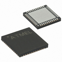
ATMEGA1284P-MUR Atmel, ATMEGA1284P-MUR Datasheet - Page 121

ATMEGA1284P-MUR
Manufacturer Part Number
ATMEGA1284P-MUR
Description
MCU AVR 128KB FLASH 20MHZ 44VQFN
Manufacturer
Atmel
Series
AVR® ATmegar
Specifications of ATMEGA1284P-MUR
Core Processor
AVR
Core Size
8-Bit
Speed
20MHz
Connectivity
I²C, SPI, UART/USART
Peripherals
Brown-out Detect/Reset, POR, PWM, WDT
Number Of I /o
32
Program Memory Size
128KB (64K x 16)
Program Memory Type
FLASH
Eeprom Size
4K x 8
Ram Size
16K x 8
Voltage - Supply (vcc/vdd)
1.8 V ~ 5.5 V
Data Converters
A/D 8x10b
Oscillator Type
Internal
Operating Temperature
-40°C ~ 85°C
Package / Case
44-VQFN Exposed Pad
For Use With
ATSTK600 - DEV KIT FOR AVR/AVR32
Lead Free Status / RoHS Status
Lead free / RoHS Compliant
Available stocks
Company
Part Number
Manufacturer
Quantity
Price
Company:
Part Number:
ATMEGA1284P-MUR
Manufacturer:
FREESCALE
Quantity:
593
- Current page: 121 of 581
- Download datasheet (27Mb)
15.7
8272A–AVR–01/10
Output Compare Units
cleared by software (writing a logical one to the I/O bit location). For measuring frequency only,
the clearing of the ICFn Flag is not required (if an interrupt handler is used).
The 16-bit comparator continuously compares TCNTn with the Output Compare Register
(OCRnx). If TCNT equals OCRnx the comparator signals a match. A match will set the Output
Compare Flag (OCFnx) at the next timer clock cycle. If enabled (OCIEnx = 1), the Output Com-
pare Flag generates an Output Compare interrupt. The OCFnx Flag is automatically cleared
when the interrupt is executed. Alternatively the OCFnx Flag can be cleared by software by writ-
ing a logical one to its I/O bit location. The Waveform Generator uses the match signal to
generate an output according to operating mode set by the Waveform Generation mode
(WGMn3:0) bits and Compare Output mode (COMnx1:0) bits. The TOP and BOTTOM signals
are used by the Waveform Generator for handling the special cases of the extreme values in
some modes of operation
A special feature of Output Compare unit A allows it to define the Timer/Counter TOP value (i.e.,
counter resolution). In addition to the counter resolution, the TOP value defines the period time
for waveforms generated by the Waveform Generator.
Figure 15-4
bit names indicates the device number (n = n for Timer/Counter n), and the “x” indicates Output
Compare unit (A/B/C). The elements of the block diagram that are not directly a part of the Out-
put Compare unit are gray shaded.
Figure 15-4. Output Compare Unit, Block Diagram
The OCRnx Register is double buffered when using any of the twelve Pulse Width Modulation
(PWM) modes. For the Normal and Clear Timer on Compare (CTC) modes of operation, the
double buffering is disabled. The double buffering synchronizes the update of the OCRnx Com-
pare Register to either TOP or BOTTOM of the counting sequence. The synchronization
164A/164PA/324A/324PA/644A/644PA/1284/1284P
shows a block diagram of the Output Compare unit. The small “n” in the register and
OCRnxH Buf. (8-bit)
(See Section “15.9” on page
OCRnxH (8-bit)
BOTTOM
OCRnx Buffer (16-bit Register)
TEMP (8-bit)
TOP
OCRnx (16-bit Register)
OCRnxL Buf. (8-bit)
OCRnxL (8-bit)
DATA BUS
Waveform Generator
WGMn3:0
=
(16-bit Comparator )
(8-bit)
124.)
COMnx1:0
TCNTnH (8-bit)
OCFnx (Int.Req.)
TCNTn (16-bit Counter)
TCNTnL (8-bit)
OCnx
121
Related parts for ATMEGA1284P-MUR
Image
Part Number
Description
Manufacturer
Datasheet
Request
R

Part Number:
Description:
Manufacturer:
ATMEL Corporation
Datasheet:

Part Number:
Description:
Microcontroller with 128K bytes In-system programmable flash, 8 MHz, power supply =2.7 - 5.5V
Manufacturer:
ATMEL Corporation
Datasheet:

Part Number:
Description:
IC AVR MCU 128K 16MHZ 5V 64TQFP
Manufacturer:
Atmel
Datasheet:

Part Number:
Description:
IC AVR MCU 128K 16MHZ 5V 64-QFN
Manufacturer:
Atmel
Datasheet:

Part Number:
Description:
IC AVR MCU 128K 16MHZ COM 64-QFN
Manufacturer:
Atmel
Datasheet:

Part Number:
Description:
IC AVR MCU 128K 16MHZ 64-TQFP
Manufacturer:
Atmel
Datasheet:

Part Number:
Description:
IC AVR MCU 128K 16MHZ 64-TQFP
Manufacturer:
Atmel
Datasheet:

Part Number:
Description:
IC AVR MCU 128K 16MHZ IND 64-QFN
Manufacturer:
Atmel
Datasheet:

Part Number:
Description:
MCU AVR 128KB FLASH 16MHZ 64TQFP
Manufacturer:
Atmel
Datasheet:

Part Number:
Description:
MCU AVR 128KB FLASH 16MHZ 64QFN
Manufacturer:
Atmel
Datasheet:

Part Number:
Description:
MCU AVR 128KB FLASH 16MHZ 64TQFP
Manufacturer:
Atmel
Datasheet:


