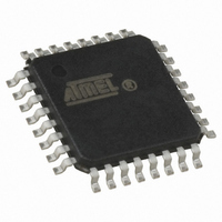
ATMEGA48A-AU Atmel, ATMEGA48A-AU Datasheet - Page 136

ATMEGA48A-AU
Manufacturer Part Number
ATMEGA48A-AU
Description
IC MCU AVR 4K FLASH 32TQFP
Manufacturer
Atmel
Series
AVR® ATmegar
Specifications of ATMEGA48A-AU
Core Processor
AVR
Core Size
8-Bit
Speed
20MHz
Connectivity
I²C, SPI, UART/USART
Peripherals
Brown-out Detect/Reset, POR, PWM, WDT
Number Of I /o
23
Program Memory Size
4KB (2K x 16)
Program Memory Type
FLASH
Eeprom Size
256 x 8
Ram Size
512 x 8
Voltage - Supply (vcc/vdd)
1.8 V ~ 5.5 V
Data Converters
A/D 8x10b
Oscillator Type
Internal
Operating Temperature
-40°C ~ 85°C
Package / Case
32-TQFP, 32-VQFP
Controller Family/series
Atmega
No. Of I/o's
23
Eeprom Memory Size
256Byte
Ram Memory Size
512Byte
Cpu Speed
20MHz
Rohs Compliant
Yes
Processor Series
ATmega
Core
AVR
Data Bus Width
8 bit
Data Ram Size
512 B
Interface Type
TWI, SPI, USART
Maximum Clock Frequency
20 MHz
Number Of Programmable I/os
23
Number Of Timers
3
Operating Supply Voltage
3.3 V
Maximum Operating Temperature
+ 85 C
Mounting Style
SMD/SMT
Minimum Operating Temperature
- 40 C
Operating Temperature Range
- 40 C to + 85 C
Lead Free Status / RoHS Status
Lead free / RoHS Compliant
Available stocks
Company
Part Number
Manufacturer
Quantity
Price
- Current page: 136 of 566
- Download datasheet (23Mb)
8271C–AVR–08/10
Table 15-2
PWM mode.
Table 15-2.
Note:
Table 15-3
correct or the phase and frequency correct, PWM mode.
Table 15-3.
Note:
• Bit 1:0 – WGM11:0: Waveform Generation Mode
Combined with the WGM13:2 bits found in the TCCR1B Register, these bits control the counting
sequence of the counter, the source for maximum (TOP) counter value, and what type of wave-
form generation to be used, see
unit are: Normal mode (counter), Clear Timer on Compare match (CTC) mode, and three types
of Pulse Width Modulation (PWM) modes.
ATmega48A/48PA/88A/88PA/168A/168PA/328/328
COM1A1/COM1B1
COM1A1/COM1B1
1. A special case occurs when OCR1A/OCR1B equals TOP and COM1A1/COM1B1 is set. In
1. A special case occurs when OCR1A/OCR1B equals TOP and COM1A1/COM1B1 is set.
0
0
1
1
0
0
1
1
this case the compare match is ignored, but the set or clear is done at BOTTOM.
“15.9.3” on page 127.
Section “15.9.4” on page 129.
shows the COM1x1:0 bit functionality when the WGM13:0 bits are set to the phase
shows the COM1x1:0 bit functionality when the WGM13:0 bits are set to the fast
Compare Output Mode, Fast PWM
Compare Output Mode, Phase Correct and Phase and Frequency Correct
PWM
(1)
COM1A0/COM1B0
COM1A0/COM1B0
for more details.
Table
0
1
0
1
0
1
0
1
15-4. Modes of operation supported by the Timer/Counter
for more details.
(See Section “15.9” on page
Description
Description
Normal port operation, OC1A/OC1B disconnected.
WGM13:0 = 9 or 11: Toggle OC1A on Compare
Match, OC1B disconnected (normal port operation).
For all other WGM1 settings, normal port operation,
OC1A/OC1B disconnected.
Clear OC1A/OC1B on Compare Match when up-
counting. Set OC1A/OC1B on Compare Match when
downcounting.
Set OC1A/OC1B on Compare Match when up-
counting. Clear OC1A/OC1B on Compare Match
when downcounting.
Normal port operation, OC1A/OC1B disconnected.
WGM13:0 = 14 or 15: Toggle OC1A on Compare
Match, OC1B disconnected (normal port operation).
For all other WGM1 settings, normal port operation,
OC1A/OC1B disconnected.
Clear OC1A/OC1B on Compare Match, set
OC1A/OC1B at BOTTOM (non-inverting mode)
Set OC1A/OC1B on Compare Match, clear
OC1A/OC1B at BOTTOM (inverting mode)
(1)
126.).
See Section
See
136
Related parts for ATMEGA48A-AU
Image
Part Number
Description
Manufacturer
Datasheet
Request
R

Part Number:
Description:
IC AVR MCU 4K 5V 20MHZ 32-TQFP
Manufacturer:
Atmel
Datasheet:

Part Number:
Description:
Manufacturer:
Atmel Corporation
Datasheet:

Part Number:
Description:
Manufacturer:
Atmel Corporation
Datasheet:

Part Number:
Description:
IC AVR MCU 4K 20MHZ 5V 32TQFP
Manufacturer:
Atmel
Datasheet:

Part Number:
Description:
IC AVR MCU 4K 20MHZ 5V 28DIP
Manufacturer:
Atmel
Datasheet:

Part Number:
Description:
IC AVR MCU 4K 20MHZ 5V 32-QFN
Manufacturer:
Atmel
Datasheet:

Part Number:
Description:
IC AVR MCU 4K 5V 20MHZ 32-TQFP
Manufacturer:
Atmel
Datasheet:

Part Number:
Description:
IC AVR MCU 4K 5V 20MHZ 32-QFN
Manufacturer:
Atmel
Datasheet:

Part Number:
Description:
IC AVR MCU 4K 5V 20MHZ 32-QFN
Manufacturer:
Atmel
Datasheet:

Part Number:
Description:
IC AVR MCU 4K 5V 20MHZ 28-DIP
Manufacturer:
Atmel
Datasheet:

Part Number:
Description:
IC AVR MCU 4K 5V 20MHZ 28-DIP
Manufacturer:
Atmel
Datasheet:

Part Number:
Description:
IC AVR MCU 4K FLASH 20MHZ 28QFN
Manufacturer:
Atmel
Datasheet:


