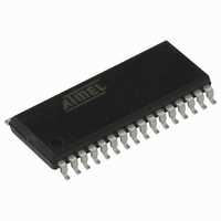
AT90PWM316-16SUR Atmel, AT90PWM316-16SUR Datasheet - Page 127

AT90PWM316-16SUR
Manufacturer Part Number
AT90PWM316-16SUR
Description
MCU AVR 16K FLASH 16MHZ 32-SOIC
Manufacturer
Atmel
Series
AVR® 90PWM Lightingr
Datasheet
1.AT90PWM216-16SU.pdf
(359 pages)
Specifications of AT90PWM316-16SUR
Core Processor
AVR
Core Size
8-Bit
Speed
16MHz
Connectivity
SPI, UART/USART
Peripherals
Brown-out Detect/Reset, POR, PWM, WDT
Number Of I /o
27
Program Memory Size
16KB (16K x 8)
Program Memory Type
FLASH
Eeprom Size
512 x 8
Ram Size
1K x 8
Voltage - Supply (vcc/vdd)
2.7 V ~ 5.5 V
Data Converters
A/D 11x10b; D/A 1x10b
Oscillator Type
Internal
Operating Temperature
-40°C ~ 105°C
Package / Case
32-SOIC (7.5mm Width)
For Use With
ATSTK600-SOIC - STK600 SOCKET/ADAPTER FOR SOICATAVRMC200 - KIT EVAL FOR AT90PWM3 ASYNCATAVRFBKIT - KIT DEMO BALLAST FOR AT90PWM2
Lead Free Status / RoHS Status
Lead free / RoHS Compliant
Available stocks
Company
Part Number
Manufacturer
Quantity
Price
- Current page: 127 of 359
- Download datasheet (6Mb)
15.10.3
7710E–AVR–08/10
Timer/Counter1 Control Register C – TCCR1C
When the ICRn is used as TOP value (see description of the WGMn3:0 bits located in the
TCCRnA and the TCCRnB Register), the ICPn is disconnected and consequently the Input Cap-
ture function is disabled.
• Bit 5 – Reserved Bit
This bit is reserved for future use. For ensuring compatibility with future devices, this bit must be
written to zero when TCCRnB is written.
• Bit 4:3 – WGMn3:2: Waveform Generation Mode
See TCCRnA Register description.
• Bit 2:0 – CSn2:0: Clock Select
The three Clock Select bits select the clock source to be used by the Timer/Counter, see
15-10
Table 15-6.
If external pin modes are used for the Timer/Countern, transitions on the Tn pin will clock the
counter even if the pin is configured as an output. This feature allows software control of the
counting.
• Bit 7 – FOCnA: Force Output Compare for Channel A
• Bit 6 – FOCnB: Force Output Compare for Channel B
The FOCnA/FOCnB bits are only active when the WGMn3:0 bits specifies a non-PWM mode.
However, for ensuring compatibility with future devices, these bits must be set to zero when
TCCRnA is written when operating in a PWM mode. When writing a logical one to the
FOCnA/FOCnB bit, an immediate compare match is forced on the Waveform Generation unit.
The OCnA/OCnB output is changed according to its COMnx1:0 bits setting. Note that the
FOCnA/FOCnB bits are implemented as strobes. Therefore it is the value present in the
COMnx1:0 bits that determine the effect of the forced compare.
Bit
Read/Write
Initial Value
CSn2
0
0
0
0
1
1
1
1
and
Figure
CSn1
0
0
1
1
0
0
1
1
Clock Select Bit Description
FOC1A
R/W
7
0
15-11.
CSn0
FOC1B
0
1
0
1
0
1
0
1
R/W
6
0
Description
No clock source (Timer/Counter stopped).
clk
clk
clk
clk
clk
External clock source on Tn pin. Clock on falling edge.
External clock source on Tn pin. Clock on rising edge.
I/O
I/O
I/O
I/O
I/O
R
5
–
0
/1 (No prescaling)
/8 (From prescaler)
/64 (From prescaler)
/256 (From prescaler)
/1024 (From prescaler)
R
4
–
0
R
3
–
0
AT90PWM216/316
R
2
–
0
R
1
–
0
R
0
–
0
TCCR1C
Figure
127
Related parts for AT90PWM316-16SUR
Image
Part Number
Description
Manufacturer
Datasheet
Request
R

Part Number:
Description:
Manufacturer:
Atmel Corporation
Datasheet:

Part Number:
Description:
MCU AVR 16K FLASH 16MHZ 32-QFN
Manufacturer:
Atmel
Datasheet:

Part Number:
Description:
MCU AVR 16K ISP FLSH 16MHZ32SOIC
Manufacturer:
Atmel
Datasheet:

Part Number:
Description:
8-bit Microcontroller with 16K Bytes In-System Programmable Flash
Manufacturer:
ATMEL [ATMEL Corporation]
Datasheet:

Part Number:
Description:
8-bit Avr Microcontroller With 16k Bytes Of Isp Flash And Usb Controller
Manufacturer:
ATMEL Corporation
Datasheet:

Part Number:
Description:
DEV KIT FOR AVR/AVR32
Manufacturer:
Atmel
Datasheet:

Part Number:
Description:
INTERVAL AND WIPE/WASH WIPER CONTROL IC WITH DELAY
Manufacturer:
ATMEL Corporation
Datasheet:

Part Number:
Description:
Low-Voltage Voice-Switched IC for Hands-Free Operation
Manufacturer:
ATMEL Corporation
Datasheet:

Part Number:
Description:
MONOLITHIC INTEGRATED FEATUREPHONE CIRCUIT
Manufacturer:
ATMEL Corporation
Datasheet:

Part Number:
Description:
AM-FM Receiver IC U4255BM-M
Manufacturer:
ATMEL Corporation
Datasheet:

Part Number:
Description:
Monolithic Integrated Feature Phone Circuit
Manufacturer:
ATMEL Corporation
Datasheet:

Part Number:
Description:
Multistandard Video-IF and Quasi Parallel Sound Processing
Manufacturer:
ATMEL Corporation
Datasheet:


