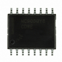
MC908QY8CDWE Freescale Semiconductor, MC908QY8CDWE Datasheet - Page 104

MC908QY8CDWE
Manufacturer Part Number
MC908QY8CDWE
Description
IC MCU 8BIT 8K FLASH 16-SOIC
Manufacturer
Freescale Semiconductor
Series
HC08r
Datasheet
1.MC908QB8CDWE.pdf
(236 pages)
Specifications of MC908QY8CDWE
Core Processor
HC08
Core Size
8-Bit
Speed
8MHz
Peripherals
LVD, POR, PWM
Number Of I /o
13
Program Memory Size
8KB (8K x 8)
Program Memory Type
FLASH
Ram Size
256 x 8
Voltage - Supply (vcc/vdd)
2.7 V ~ 5.5 V
Data Converters
A/D 4x10b
Oscillator Type
External
Operating Temperature
-40°C ~ 85°C
Package / Case
16-SOIC (0.300", 7.5mm Width)
Processor Series
HC08QY
Core
HC08
Data Bus Width
8 bit
Data Ram Size
256 B
Maximum Clock Frequency
8 MHz
Number Of Programmable I/os
13
Number Of Timers
2
Operating Supply Voltage
3 V to 5 V
Maximum Operating Temperature
+ 85 C
Mounting Style
SMD/SMT
Development Tools By Supplier
FSICEBASE, M68CBL05AE, DEMO908QB8, DEMO908QC16
Minimum Operating Temperature
- 40 C
On-chip Adc
4-ch x 10-bit
Lead Free Status / RoHS Status
Lead free / RoHS Compliant
Eeprom Size
-
Connectivity
-
Lead Free Status / Rohs Status
Lead free / RoHS Compliant
Available stocks
Company
Part Number
Manufacturer
Quantity
Price
Company:
Part Number:
MC908QY8CDWE
Manufacturer:
Winbond
Quantity:
16 700
Part Number:
MC908QY8CDWE
Manufacturer:
FREESCALE
Quantity:
20 000
- Current page: 104 of 236
- Download datasheet (3Mb)
Input/Output Ports (PORTS)
12.2.1 Port A Data Register
The port A data register (PTA) contains a data latch for each of the six port A pins.
PTA[5:0] — Port A Data Bits
AWUL — Auto Wakeup Latch Data Bit
12.2.2 Data Direction Register A
Data direction register A (DDRA) determines whether each port A pin is an input or an output. Writing a 1
to a DDRA bit enables the output buffer for the corresponding port A pin; a 0 disables the output buffer.
DDRA[5:0] — Data Direction Register A Bits
Figure 12-3
104
These read/write bits are software programmable. Data direction of each port A pin is under the control
of the corresponding bit in data direction register A. Reset has no effect on port A data.
This is a read-only bit which has the value of the auto wakeup interrupt request latch. The wakeup
request signal is generated internally (see
port nor any of the associated bits such as PTA6 data register, pullup enable or direction. .
These read/write bits control port A data direction. Reset clears DDRA[5:0], configuring all port A pins
as inputs.
1 = Corresponding port A pin configured as output
0 = Corresponding port A pin configured as input
shows the port A I/O logic.
Reset:
Reset:
Read:
Write:
Read:
Write:
Avoid glitches on port A pins by writing to the port A data register before
changing data direction register A bits from 0 to 1.
Bit 7
Bit 7
R
R
R
0
Figure 12-2. Data Direction Register A (DDRA)
= Unimplemented
= Reserved
AWUL
Figure 12-1. Port A Data Register (PTA)
R
6
6
0
MC68HC908QB8 Data Sheet, Rev. 3
DDRA5
PTA5
5
5
0
Chapter 4 Auto Wakeup Module
DDRA4
Unaffected by reset
PTA4
NOTE
4
4
0
= Unimplemented
DDRA3
PTA3
3
3
0
PTA2
2
2
0
0
DDRA1
PTA1
1
1
0
(AWU)). There is no PTA6
Freescale Semiconductor
DDRA0
PTA0
Bit 0
Bit 0
0
Related parts for MC908QY8CDWE
Image
Part Number
Description
Manufacturer
Datasheet
Request
R
Part Number:
Description:
Manufacturer:
Freescale Semiconductor, Inc
Datasheet:
Part Number:
Description:
Manufacturer:
Freescale Semiconductor, Inc
Datasheet:
Part Number:
Description:
Manufacturer:
Freescale Semiconductor, Inc
Datasheet:
Part Number:
Description:
Manufacturer:
Freescale Semiconductor, Inc
Datasheet:
Part Number:
Description:
Manufacturer:
Freescale Semiconductor, Inc
Datasheet:
Part Number:
Description:
Manufacturer:
Freescale Semiconductor, Inc
Datasheet:
Part Number:
Description:
Manufacturer:
Freescale Semiconductor, Inc
Datasheet:
Part Number:
Description:
Manufacturer:
Freescale Semiconductor, Inc
Datasheet:
Part Number:
Description:
Manufacturer:
Freescale Semiconductor, Inc
Datasheet:
Part Number:
Description:
Manufacturer:
Freescale Semiconductor, Inc
Datasheet:
Part Number:
Description:
Manufacturer:
Freescale Semiconductor, Inc
Datasheet:
Part Number:
Description:
Manufacturer:
Freescale Semiconductor, Inc
Datasheet:
Part Number:
Description:
Manufacturer:
Freescale Semiconductor, Inc
Datasheet:
Part Number:
Description:
Manufacturer:
Freescale Semiconductor, Inc
Datasheet:
Part Number:
Description:
Manufacturer:
Freescale Semiconductor, Inc
Datasheet:


