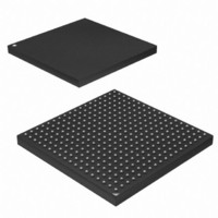
AT91SAM9M10-CU Atmel, AT91SAM9M10-CU Datasheet - Page 573

AT91SAM9M10-CU
Manufacturer Part Number
AT91SAM9M10-CU
Description
IC MCU 16/32BIT ARM9 324TFBGA
Manufacturer
Atmel
Series
AT91SAMr
Specifications of AT91SAM9M10-CU
Core Processor
ARM9
Core Size
16/32-Bit
Speed
400MHz
Connectivity
EBI/EMI, Ethernet, I²C, SPI, SSC, UART/USART, USB
Peripherals
AC'97, DMA, LCD, POR, PWM, WDT
Number Of I /o
160
Program Memory Size
64KB (64K x 8)
Program Memory Type
ROM
Ram Size
128K x 8
Voltage - Supply (vcc/vdd)
0.9 V ~ 1.1 V
Data Converters
A/D 8x10b
Oscillator Type
Internal
Operating Temperature
-40°C ~ 85°C
Package / Case
324-TFBGA
Processor Series
AT91SAMx
Core
ARM926EJ-S
Data Bus Width
32 bit
Data Ram Size
32 KB
Interface Type
2-Wire, SPI, USART
Maximum Clock Frequency
133 MHz
Number Of Programmable I/os
5
Number Of Timers
2 x 16 bit
Operating Supply Voltage
1.65 V to 3.6 V
Maximum Operating Temperature
+ 85 C
Mounting Style
SMD/SMT
3rd Party Development Tools
JTRACE-ARM-2M, MDK-ARM, RL-ARM, ULINK2
Development Tools By Supplier
AT91SAM-ICE, AT91-ISP, AT91SAM9M10-G45-EK
Controller Family/series
AT91
No. Of I/o's
160
Ram Memory Size
64KB
Cpu Speed
400MHz
No. Of Timers
2
Rohs Compliant
Yes
Cpu Family
AT91
Device Core
ARM926EJ-S
Device Core Size
32b
Frequency (max)
400MHz
Total Internal Ram Size
64KB
# I/os (max)
160
Number Of Timers - General Purpose
7
Operating Supply Voltage (typ)
1.8/2.5/3.3V
Operating Supply Voltage (max)
1.1/1.95/3.6V
Operating Supply Voltage (min)
0.9/1.65/1.8/3V
On-chip Adc
8-chx10-bit
Instruction Set Architecture
RISC
Operating Temp Range
-40C to 85C
Operating Temperature Classification
Industrial
Mounting
Surface Mount
Pin Count
324
Package Type
TFBGA
Lead Free Status / RoHS Status
Lead free / RoHS Compliant
Eeprom Size
-
Lead Free Status / Rohs Status
Lead free / RoHS Compliant
Available stocks
Company
Part Number
Manufacturer
Quantity
Price
Company:
Part Number:
AT91SAM9M10-CU
Manufacturer:
Atmel
Quantity:
996
- Current page: 573 of 1404
- Download datasheet (22Mb)
32.7.8.12
Figure 32-45. Frame Slot Mode
6355B–ATARM–21-Jun-10
TXRDY
Write
US_LINID
Write
US_THR
LINTC
Break
Frame Slot Mode
Header
Synch
This mode is useful only for Master nodes. It respects the following rule: each frame slot shall be
longer than or equal to TFrame_Maximum.
If the Frame Slot Mode is enabled (FSDIS = 0) and a frame transfer has been completed, the
TXRDY flag is set again only after TFrame_Maximum delay, from the start of frame. So the Mas-
ter node cannot send a new header if the frame slot duration of the previous frame is inferior to
TFrame_Maximum.
If the Frame Slot Mode is disabled (FDIS = 1) and a frame transfer has been completed, the
TXRDY flag is set again immediately.
The TFrame_Maximum is calculated as below:
If the Checksum is sent (CHKDIS = 0):
If the Checksum is not sent (CHKDIS = 1):
Note:
• THeader_Nominal = 34 x TBit
• TResponse_Nominal = 10 x (NData + 1) x TBit
• TFrame_Maximum = 1.4 x (THeader_Nominal + TResponse_Nominal + 1)
• TFrame_Maximum = 1.4 x (34 + 10 x (DLC + 1 + 1) + 1) x TBIT
• TFrame_Maximum = (77 + 14 x DLC) x TBIT
• THeader_Nominal = 34 x TBit
• TResponse_Nominal = 10 x NData x TBit
• TFrame_Maximum = 1.4 x (THeader_Nominal + TResponse_Nominal + 1
• TFrame_Maximum = 1.4 x (34 + 10 x (DLC + 1) + 1) x TBIT
• TFrame_Maximum = (63 + 14 x DLC) x TBIT
Data 1
The term “+1” leads to an integer result for TFrame_Max (LIN Specification 1.3)
Protected
Identifier
Data3
Frame slot = TFrame_Maximum
Response
space
Data 2
Frame
Data 1
Data 3
Data N
Response
Data N-1
Data N
AT91SAM9M10
Frame Slot Mode
Checksum
Disabled
(Note:)
(Note:)
)
Frame Slot Mode
frame
space
Inter-
Enabled
573
Related parts for AT91SAM9M10-CU
Image
Part Number
Description
Manufacturer
Datasheet
Request
R

Part Number:
Description:
MCU, MPU & DSP Development Tools KICKSTART KIT FOR AT91SAM9 PLUS
Manufacturer:
IAR Systems

Part Number:
Description:
DEV KIT FOR AVR/AVR32
Manufacturer:
Atmel
Datasheet:

Part Number:
Description:
INTERVAL AND WIPE/WASH WIPER CONTROL IC WITH DELAY
Manufacturer:
ATMEL Corporation
Datasheet:

Part Number:
Description:
Low-Voltage Voice-Switched IC for Hands-Free Operation
Manufacturer:
ATMEL Corporation
Datasheet:

Part Number:
Description:
MONOLITHIC INTEGRATED FEATUREPHONE CIRCUIT
Manufacturer:
ATMEL Corporation
Datasheet:

Part Number:
Description:
AM-FM Receiver IC U4255BM-M
Manufacturer:
ATMEL Corporation
Datasheet:

Part Number:
Description:
Monolithic Integrated Feature Phone Circuit
Manufacturer:
ATMEL Corporation
Datasheet:

Part Number:
Description:
Multistandard Video-IF and Quasi Parallel Sound Processing
Manufacturer:
ATMEL Corporation
Datasheet:

Part Number:
Description:
High-performance EE PLD
Manufacturer:
ATMEL Corporation
Datasheet:

Part Number:
Description:
8-bit Flash Microcontroller
Manufacturer:
ATMEL Corporation
Datasheet:

Part Number:
Description:
2-Wire Serial EEPROM
Manufacturer:
ATMEL Corporation
Datasheet:


