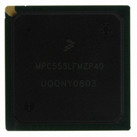
MPC555LFMZP40 Freescale Semiconductor, MPC555LFMZP40 Datasheet - Page 673

MPC555LFMZP40
Manufacturer Part Number
MPC555LFMZP40
Description
IC MCU 32BIT 40MHZ 272-BGA
Manufacturer
Freescale Semiconductor
Series
MPC5xxr
Datasheets
1.MPC555LFMZP40.pdf
(12 pages)
2.MPC555LFMZP40.pdf
(966 pages)
3.MPC555LFMZP40.pdf
(3 pages)
Specifications of MPC555LFMZP40
Core Processor
PowerPC
Core Size
32-Bit
Speed
40MHz
Connectivity
CAN, EBI/EMI, SCI, SPI, UART/USART
Peripherals
POR, PWM, WDT
Number Of I /o
101
Program Memory Size
448KB (448K x 8)
Program Memory Type
FLASH
Ram Size
26K x 8
Voltage - Supply (vcc/vdd)
2.5 V ~ 2.7 V
Data Converters
A/D 32x10b
Oscillator Type
External
Operating Temperature
-40°C ~ 125°C
Package / Case
272-PBGA
Controller Family/series
POWER 5xx
Ram Memory Size
26KB
Cpu Speed
63MIPS
Embedded Interface Type
QSPI, SCI, TouCAN
Operating Temperature Range
-40°C To +125°C
No. Of Pins
272
Rohs Compliant
No
Processor Series
MPC5xx
Core
PowerPC
Data Bus Width
32 bit
Data Ram Size
26 KB
Interface Type
CAN, QSPI, SCI
Maximum Clock Frequency
40 MHz
Number Of Programmable I/os
101
Operating Supply Voltage
3.3 V to 5 V
Maximum Operating Temperature
+ 125 C
Mounting Style
SMD/SMT
Development Tools By Supplier
MPC555CMEE
Minimum Operating Temperature
- 85 C
On-chip Adc
10 bit, 32 Channel
Cpu Family
MPC55xx
Device Core
PowerPC
Device Core Size
32b
Frequency (max)
40MHz
Total Internal Ram Size
32KB
# I/os (max)
101
Operating Supply Voltage (typ)
5V
Instruction Set Architecture
RISC
Operating Temp Range
-40C to 85C
Operating Temperature Classification
Industrial
Mounting
Surface Mount
Pin Count
272
Package Type
BGA
For Use With
MPC555CMEE - KIT EVAL FOR MPC555
Lead Free Status / RoHS Status
Contains lead / RoHS non-compliant
Eeprom Size
-
Lead Free Status / Rohs Status
No
Available stocks
Company
Part Number
Manufacturer
Quantity
Price
Company:
Part Number:
MPC555LFMZP40
Manufacturer:
MOTOLOLA
Quantity:
853
Company:
Part Number:
MPC555LFMZP40
Manufacturer:
Freescale Semiconductor
Quantity:
10 000
Company:
Part Number:
MPC555LFMZP40R2
Manufacturer:
Freescale Semiconductor
Quantity:
10 000
- Current page: 673 of 966
- Download datasheet (15Mb)
MPC555
USER’S MANUAL
State
S1
S2
S3
S4
Normal Operation:
Normal array reads and register accesses. The
block protect information and pulse width timing
control can be modified.
First Program Hardware Interlock Write:
Normal read operation still occurs. The array will
accept programming writes. Accesses to the regis-
ters are normal register accesses. A write to CM-
FCTL can not change EHV at this time. If the write
is to a register, no data is stored in the program
page buffers, and the CMF remains in state S2.
Expanded Program Hardware Interlock Operation:
Program margin reads will occur. Programming
writes are accepted so that all program pages may
be programmed. These writes may be to any CMF
array location. The program page buffers will be
updated using only the data, the lower address
(ADDR[26:29]) and the block address. Accesses to
the registers are normal register accesses. A write
to CMFCTL can change EHV. If the write is to a
register, no data is stored in the program page buff-
er.
Program Operation:
High voltage is applied to the array or shadow in-
formation to program the CMF bit cells. The pulse
width timer is active if SCLKR[0:2] ≠ 0 and HVS
can be polled to time the program pulse. No further
programming writes are accepted. During pro-
gramming the array does not respond to any ac-
cess. Accesses to the registers are allowed. A
write to CMFCTL can change EHV only.
/
MPC556
Table 19-9 Program Interlock State Descriptions
Freescale Semiconductor, Inc.
Mode
For More Information On This Product,
CDR MoneT FLASH EEPROM
Go to: www.freescale.com
Rev. 15 October 2000
State
Next
S2
S1
S3
S1
S4
S1
S5
T2
T1
T3
T6
T4
T7
T5
Write PE = 0, SES = 1
Write SES = 0 or a master reset
Hardware Interlock
A successful write to any CMF array lo-
cation. This programming write latches
the selected word of data into the pro-
gramming page buffer and the address
is latched to select the location to be
programmed. Once a bit has been writ-
ten then it will remain in the program
buffer until another write to the word or
a write of SES = 0 or a program margin
read determines that the state of the bit
needs no further modification by the
program operation. If the write is to a
register no data will be stored in the
program page buffers and the CMF will
remain in state S2.
Write SES = 0 or a master reset
Write EHV = 1
Master reset
Write EHV = 0, disable the internal
memory map or a soft reset.
Transition Requirement
MOTOROLA
19-21
Related parts for MPC555LFMZP40
Image
Part Number
Description
Manufacturer
Datasheet
Request
R
Part Number:
Description:
Manufacturer:
Freescale Semiconductor, Inc
Datasheet:
Part Number:
Description:
Manufacturer:
Freescale Semiconductor, Inc
Datasheet:
Part Number:
Description:
Manufacturer:
Freescale Semiconductor, Inc
Datasheet:
Part Number:
Description:
Manufacturer:
Freescale Semiconductor, Inc
Datasheet:
Part Number:
Description:
Manufacturer:
Freescale Semiconductor, Inc
Datasheet:
Part Number:
Description:
Manufacturer:
Freescale Semiconductor, Inc
Datasheet:
Part Number:
Description:
Manufacturer:
Freescale Semiconductor, Inc
Datasheet:
Part Number:
Description:
Manufacturer:
Freescale Semiconductor, Inc
Datasheet:
Part Number:
Description:
Manufacturer:
Freescale Semiconductor, Inc
Datasheet:
Part Number:
Description:
Manufacturer:
Freescale Semiconductor, Inc
Datasheet:
Part Number:
Description:
Manufacturer:
Freescale Semiconductor, Inc
Datasheet:
Part Number:
Description:
Manufacturer:
Freescale Semiconductor, Inc
Datasheet:
Part Number:
Description:
Manufacturer:
Freescale Semiconductor, Inc
Datasheet:
Part Number:
Description:
Manufacturer:
Freescale Semiconductor, Inc
Datasheet:
Part Number:
Description:
Manufacturer:
Freescale Semiconductor, Inc
Datasheet:


