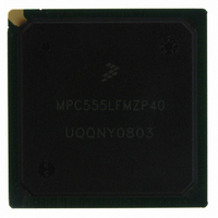
MPC555LFMZP40 Freescale Semiconductor, MPC555LFMZP40 Datasheet - Page 565

MPC555LFMZP40
Manufacturer Part Number
MPC555LFMZP40
Description
IC MCU 32BIT 40MHZ 272-BGA
Manufacturer
Freescale Semiconductor
Series
MPC5xxr
Datasheets
1.MPC555LFMZP40.pdf
(12 pages)
2.MPC555LFMZP40.pdf
(966 pages)
3.MPC555LFMZP40.pdf
(3 pages)
Specifications of MPC555LFMZP40
Core Processor
PowerPC
Core Size
32-Bit
Speed
40MHz
Connectivity
CAN, EBI/EMI, SCI, SPI, UART/USART
Peripherals
POR, PWM, WDT
Number Of I /o
101
Program Memory Size
448KB (448K x 8)
Program Memory Type
FLASH
Ram Size
26K x 8
Voltage - Supply (vcc/vdd)
2.5 V ~ 2.7 V
Data Converters
A/D 32x10b
Oscillator Type
External
Operating Temperature
-40°C ~ 125°C
Package / Case
272-PBGA
Controller Family/series
POWER 5xx
Ram Memory Size
26KB
Cpu Speed
63MIPS
Embedded Interface Type
QSPI, SCI, TouCAN
Operating Temperature Range
-40°C To +125°C
No. Of Pins
272
Rohs Compliant
No
Processor Series
MPC5xx
Core
PowerPC
Data Bus Width
32 bit
Data Ram Size
26 KB
Interface Type
CAN, QSPI, SCI
Maximum Clock Frequency
40 MHz
Number Of Programmable I/os
101
Operating Supply Voltage
3.3 V to 5 V
Maximum Operating Temperature
+ 125 C
Mounting Style
SMD/SMT
Development Tools By Supplier
MPC555CMEE
Minimum Operating Temperature
- 85 C
On-chip Adc
10 bit, 32 Channel
Cpu Family
MPC55xx
Device Core
PowerPC
Device Core Size
32b
Frequency (max)
40MHz
Total Internal Ram Size
32KB
# I/os (max)
101
Operating Supply Voltage (typ)
5V
Instruction Set Architecture
RISC
Operating Temp Range
-40C to 85C
Operating Temperature Classification
Industrial
Mounting
Surface Mount
Pin Count
272
Package Type
BGA
For Use With
MPC555CMEE - KIT EVAL FOR MPC555
Lead Free Status / RoHS Status
Contains lead / RoHS non-compliant
Eeprom Size
-
Lead Free Status / Rohs Status
No
Available stocks
Company
Part Number
Manufacturer
Quantity
Price
Company:
Part Number:
MPC555LFMZP40
Manufacturer:
MOTOLOLA
Quantity:
853
Company:
Part Number:
MPC555LFMZP40
Manufacturer:
Freescale Semiconductor
Quantity:
10 000
Company:
Part Number:
MPC555LFMZP40R2
Manufacturer:
Freescale Semiconductor
Quantity:
10 000
- Current page: 565 of 966
- Download datasheet (15Mb)
MPC555
USER’S MANUAL
Bit(s)
8:15
POL
6:7
0
1
2
3
4
5
0
0
0
1
1
1
Control Bits
/
MPC556
Name
FREN
TRSP
DDR
POL
EN
PIN
EN
CP
0
0
1
0
0
1
—
Table 15-24 PWMSM Output Pin Polarity Selection
Pin input status. The PIN bit reflects the state present on the MPWMSM pin. The software can
thus monitor the signal on the pin.
The PIN bit is a read-only bit. Writing to the PIN bit has no effect.
Data direction register. The DDR bit indicates the direction for the pin when the PWM function
is not used (disable mode). Note that when the PWM function is used, the DDR bit has no effect.
Table 15-24
direction register (DDR) bit.
0 = Pin is an input.
1 = Pin is an output.
Freeze enable. This active high read/write control bit enables the MPWMSM to recognize the
freeze signal on the MIOB.
0 = MPWMSM not frozen even if the MIOB freeze line is active.
1 = MPWMSM frozen if the MIOB freeze line is active.
Transparent mode. The TRSP bit indicates that the MPWMSM double buffers are transparent:
when the software writes to either the MPWMA or MPWMB1 register the value written is imme-
diately transferred to respectively the counter or register MPWMB2.
0 = Transparent mode de-activated.
1 = Transparent mode activated.
Output polarity control. The POL bit works in conjunction with the EN bit and controls whether
the MPWMSM drives the pin with the true or the inverted value of the output flip-flop
Table 15-24
direction register (DDR) bit.
Enable PWM signal generation. The EN bit defines whether the MPWMSM generates a PWM
signal or is used as an I/O channel:
Table 15-24
direction register (DDR) bit.
0 = PWM generation disabled (pin can be used as I/O).
1 = PWM generation enabled (pin is output only).
Reserved
Clock Prescaler. This 8-bit read/write register stores the two’s complement of the desired mod-
ulus value for loading into the built-in 8-bit clock prescaler. The value loaded defines the divide
ratio for the signal that clocks the MPWMSM period counter.
ratio according to the CP values.
DDR
—
—
0
1
0
1
Table 15-23 MPWMSMSCR Bit Descriptions
MODULAR INPUT/OUTPUT SUBSYSTEM (MIOS1)
Freescale Semiconductor, Inc.
Pin Direction
For More Information On This Product,
lists the different uses for the polarity (POL) bit, the enable (EN) bit and the data
lists the different uses for the polarity (POL) bit, the enable (EN) bit and the data
lists the different uses for the polarity (POL) bit, the enable (EN) bit and the data
(I/O)
O
O
O
O
I
I
Go to: www.freescale.com
Rev. 15 October 2000
Always High
Always Low
High Pulse
Low Pulse
Pin State
Input
Input
Description
Falling Edge
Rising Edge
Periodic
Edge
—
—
—
—
Table 15-15
Falling Edge
Rising Edge
Variable
Edge
—
—
—
—
gives the clock divide
Interrupt On
Falling Edge
Rising Edge
MOTOROLA
Optional
—
—
—
—
15-29
Related parts for MPC555LFMZP40
Image
Part Number
Description
Manufacturer
Datasheet
Request
R
Part Number:
Description:
Manufacturer:
Freescale Semiconductor, Inc
Datasheet:
Part Number:
Description:
Manufacturer:
Freescale Semiconductor, Inc
Datasheet:
Part Number:
Description:
Manufacturer:
Freescale Semiconductor, Inc
Datasheet:
Part Number:
Description:
Manufacturer:
Freescale Semiconductor, Inc
Datasheet:
Part Number:
Description:
Manufacturer:
Freescale Semiconductor, Inc
Datasheet:
Part Number:
Description:
Manufacturer:
Freescale Semiconductor, Inc
Datasheet:
Part Number:
Description:
Manufacturer:
Freescale Semiconductor, Inc
Datasheet:
Part Number:
Description:
Manufacturer:
Freescale Semiconductor, Inc
Datasheet:
Part Number:
Description:
Manufacturer:
Freescale Semiconductor, Inc
Datasheet:
Part Number:
Description:
Manufacturer:
Freescale Semiconductor, Inc
Datasheet:
Part Number:
Description:
Manufacturer:
Freescale Semiconductor, Inc
Datasheet:
Part Number:
Description:
Manufacturer:
Freescale Semiconductor, Inc
Datasheet:
Part Number:
Description:
Manufacturer:
Freescale Semiconductor, Inc
Datasheet:
Part Number:
Description:
Manufacturer:
Freescale Semiconductor, Inc
Datasheet:
Part Number:
Description:
Manufacturer:
Freescale Semiconductor, Inc
Datasheet:


