PXAS37KBBE,557 NXP Semiconductors, PXAS37KBBE,557 Datasheet - Page 9
PXAS37KBBE,557
Manufacturer Part Number
PXAS37KBBE,557
Description
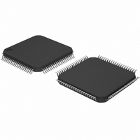
IC XA MCU 16BIT 32K OTP 80-LQFP
Manufacturer
NXP Semiconductors
Series
XAr
Datasheet
1.PXAS30KBA512.pdf
(52 pages)
Specifications of PXAS37KBBE,557
Core Processor
XA
Core Size
16-Bit
Speed
30MHz
Connectivity
EBI/EMI, I²C, UART/USART
Peripherals
PWM, WDT
Number Of I /o
50
Program Memory Size
32KB (32K x 8)
Program Memory Type
OTP
Ram Size
1K x 8
Voltage - Supply (vcc/vdd)
2.7 V ~ 5.5 V
Data Converters
A/D 8x8b
Oscillator Type
External
Operating Temperature
0°C ~ 70°C
Package / Case
80-LQFP
Processor Series
PXAS3x
Core
80C51
Data Bus Width
16 bit
Data Ram Size
1 KB
Interface Type
I2C, UART
Maximum Clock Frequency
30 MHz
Number Of Programmable I/os
50
Number Of Timers
3
Operating Supply Voltage
2.7 V to 5.5 V
Maximum Operating Temperature
+ 70 C
Mounting Style
SMD/SMT
Minimum Operating Temperature
0 C
On-chip Adc
8 bit, 8 Channel
Lead Free Status / RoHS Status
Lead free / RoHS Compliant
Eeprom Size
-
Lead Free Status / Rohs Status
Details
Other names
568-3537
935262379557
PXAS37KBBE
935262379557
PXAS37KBBE
Available stocks
Company
Part Number
Manufacturer
Quantity
Price
Company:

Part Number:
PXAS37KBBE,557
Manufacturer:
NXP Semiconductors
Quantity:
10 000


Philips Semiconductors
Table 1. Special Function Registers
2000 Dec 01
ADCON#* A/D control register
ADCS#*
ADCFG#
ADRSH0# A/D high byte result, channel 0
ADRSH1# A/D high byte result, channel 1
ADRSH2# A/D high byte result, channel 2
ADRSH3# A/D high byte result, channel 3
ADRSH4# A/D high byte result, channel 4
ADRSH5# A/D high byte result, channel 5
ADRSH6# A/D high byte result, channel 6
ADRSH7# A/D high byte result, channel 7
ADRSL#
BCR#
BTRH
BTRL
CCON#*
CMOD#
CH#
CL#
CCAPM0# PCA module 0 mode
CCAPM1# PCA module 1 mode
MNEMONIC
MNEMONIC
P5.0 – P5.7
P6.0 – P6.7
XA 16-bit microcontroller
32 K/1 K OTP/ROM/ROMless, 8-channel 8-bit A/D, low voltage (2.7 V–5.5 V),
I
NAME
2
C, 2 UARTs, 16 MB address range
A/D channel select register
A/D timing configuration
Two LSBs of 10-bit A/D result
Bus configuration register
Bus timing register high byte
Bus timing register low byte
PCA counter control
PCA mode control
PCA counter high byte
PCA counter low byte
PLCC
23–30
43, 44
PIN NUMBER
23
24
25
26
27
28
29
30
43
44
DESCRIPTION
17–20,
22–25
40, 41
LQFP
17
18
19
20
22
23
24
25
40
41
TYPE
TYPE
I/O
I/O
I/O
I/O
O
O
I
I
I
I
I
I
Address
SFR
43E
43F
4B9
4B0
4B1
4B2
4B3
4B4
4B5
4B6
4B7
4B8
46A
469
468
41A
490
48B
48A
491
492
Port 5: Port 5 is an 8-bit I/O port with a user-configurable output type. Port 5 latches have
1s written to them and are configured in the quasi-bidirectional mode during reset. The
operation of Port 5 pins as inputs and outputs depends upon the port configuration
selected. Each port pin is configured independently. Refer to the section on I/O port
configuration and the DC Electrical Characteristics for details.
Port 5 also provides various special functions as described below. Port 5 pins used as A/D
inputs must be configured by the user to the high impedance mode.
Port 6: Port 6 is a 2-bit I/O port with a user-configurable output type. Port 6 latches have
1s written to them and are configured in the quasi-bidirectional mode during reset. The
operation of Port 6 pins as inputs and outputs depends upon the port configuration
selected. Each port pin is configured independently. Refer to the section on I/O port
configuration and the DC Electrical Characteristics for details.
Port 6 also provides special functions as described below:
AD0 (P5.0):
AD1 (P5.1):
AD2 (P5.2):
AD3 (P5.3):
AD4 (P5.4):
AD5 (P5.5):
AD6/SCL (P5.6):
AD7/SDA (P5.7):
A22 (P6.0):
A23 (P6.1):
ADCS7
WM1
CIDL
MSB
DW1
3FF
2D7
3F7
CF
–
–
–
–
–
ECOM0 CAPP0 CAPN0
ECOM1 CAPP1 CAPN1
ADCS6
WDTE
DW0
WM0
3FE
2D6
3F6
CR
9
–
–
–
BIT FUNCTIONS AND ADDRESSES
ADCS5
A/D channel 0 input.
A/D channel 1 input.
A/D channel 2 input.
A/D channel 3 input.
A/D channel 4 input.
A/D channel 5 input.
A/D channel 6 input. I
A/D channel 7 input. I
Address bit 22 of the external address bus.
Address bit 23 of the external address bus.
DWA1
ALEW
CLKD
3FD
3F5
2D5
–
–
–
–
NAME AND FUNCTION
NAME AND FUNCTION
ADCS4
WAITD
DWA0
CCF4
3FC
2D4
3F4
–
–
–
–
ADRES
ADCS3
BUSD
CCF3
MAT0
MAT1
DR1
CR1
3F3
3FB
2D3
2
2
–
C serial clock input/output.
C serial data input/output.
A/D Timing Configuration
ADMOD
ADCS2
CCF2
CPS1
TOG0
TOG1
DR0
CR0
BC2
2D2
3F2
3FA
ADSST
ADCS1
PWM0
PWM1
DRA1
CRA1
CCF1
CPS0
BC1
2D1
3F1
3F9
Preliminary specification
ECCF0 00h
ECCF1 00h
ADCS0
ADINT
DRA0
CRA0
CCF0
LSB
ECF
BC0
2D0
3F0
3F8
XA-S3
00h
00h
0Fh
xx
xx
xx
xx
xx
xx
xx
xx
xx
Note 1
FFh
EFh
00h
00h
00h
00h
Reset
Value
Related parts for PXAS37KBBE,557
Image
Part Number
Description
Manufacturer
Datasheet
Request
R

Part Number:
Description:
NXP Semiconductors designed the LPC2420/2460 microcontroller around a 16-bit/32-bitARM7TDMI-S CPU core with real-time debug interfaces that include both JTAG andembedded trace
Manufacturer:
NXP Semiconductors
Datasheet:

Part Number:
Description:
NXP Semiconductors designed the LPC2458 microcontroller around a 16-bit/32-bitARM7TDMI-S CPU core with real-time debug interfaces that include both JTAG andembedded trace
Manufacturer:
NXP Semiconductors
Datasheet:
Part Number:
Description:
NXP Semiconductors designed the LPC2468 microcontroller around a 16-bit/32-bitARM7TDMI-S CPU core with real-time debug interfaces that include both JTAG andembedded trace
Manufacturer:
NXP Semiconductors
Datasheet:
Part Number:
Description:
NXP Semiconductors designed the LPC2470 microcontroller, powered by theARM7TDMI-S core, to be a highly integrated microcontroller for a wide range ofapplications that require advanced communications and high quality graphic displays
Manufacturer:
NXP Semiconductors
Datasheet:
Part Number:
Description:
NXP Semiconductors designed the LPC2478 microcontroller, powered by theARM7TDMI-S core, to be a highly integrated microcontroller for a wide range ofapplications that require advanced communications and high quality graphic displays
Manufacturer:
NXP Semiconductors
Datasheet:
Part Number:
Description:
The Philips Semiconductors XA (eXtended Architecture) family of 16-bit single-chip microcontrollers is powerful enough to easily handle the requirements of high performance embedded applications, yet inexpensive enough to compete in the market for hi
Manufacturer:
NXP Semiconductors
Datasheet:
Part Number:
Description:
The XA-S3 device is a member of Philips Semiconductors? XA(eXtended Architecture) family of high performance 16-bitsingle-chip microcontrollers
Manufacturer:
NXP Semiconductors
Datasheet:

Part Number:
Description:
The NXP BlueStreak LH75401/LH75411 family consists of two low-cost 16/32-bit System-on-Chip (SoC) devices
Manufacturer:
NXP Semiconductors
Datasheet:
Part Number:
Description:
The NXP LPC3130/3131 combine an 180 MHz ARM926EJ-S CPU core, high-speed USB2
Manufacturer:
NXP Semiconductors
Datasheet:
Part Number:
Description:
The NXP LPC3141 combine a 270 MHz ARM926EJ-S CPU core, High-speed USB 2
Manufacturer:
NXP Semiconductors
Part Number:
Description:
The NXP LPC3143 combine a 270 MHz ARM926EJ-S CPU core, High-speed USB 2
Manufacturer:
NXP Semiconductors

Part Number:
Description:
The NXP LPC3152 combines an 180 MHz ARM926EJ-S CPU core, High-speed USB 2
Manufacturer:
NXP Semiconductors
Part Number:
Description:
The NXP LPC3154 combines an 180 MHz ARM926EJ-S CPU core, High-speed USB 2
Manufacturer:
NXP Semiconductors

Part Number:
Description:
Standard level N-channel enhancement mode Field-Effect Transistor (FET) in a plastic package using NXP High-Performance Automotive (HPA) TrenchMOS technology
Manufacturer:
NXP Semiconductors
Datasheet: