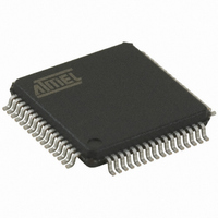
AT89C51CC03U-RDRIM Atmel, AT89C51CC03U-RDRIM Datasheet - Page 6

AT89C51CC03U-RDRIM
Manufacturer Part Number
AT89C51CC03U-RDRIM
Description
IC 8051 MCU FLASH 64K 64VQFP
Manufacturer
Atmel
Series
AT89C CANr
Datasheets
1.AT89C51CC03C-S3RIM.pdf
(198 pages)
2.AT89C51CC03C-S3RIM.pdf
(32 pages)
3.AT89C51CC03C-S3RIM.pdf
(27 pages)
4.AT89C51CC03C-S3RIM.pdf
(184 pages)
Specifications of AT89C51CC03U-RDRIM
Core Processor
8051
Core Size
8-Bit
Speed
40MHz
Connectivity
CAN, SPI, UART/USART
Peripherals
POR, PWM, WDT
Number Of I /o
36
Program Memory Size
64KB (64K x 8)
Program Memory Type
FLASH
Eeprom Size
2K x 8
Ram Size
2.25K x 8
Voltage - Supply (vcc/vdd)
3 V ~ 5.5 V
Data Converters
A/D 8x10b
Oscillator Type
External
Operating Temperature
-40°C ~ 85°C
Package / Case
64-TQFP, 64-VQFP
Lead Free Status / RoHS Status
Contains lead / RoHS non-compliant
Other names
AT89C51CC03URDRTR
Available stocks
Company
Part Number
Manufacturer
Quantity
Price
- AT89C51CC03C-S3RIM PDF datasheet
- AT89C51CC03C-S3RIM PDF datasheet #2
- AT89C51CC03C-S3RIM PDF datasheet #3
- AT89C51CC03C-S3RIM PDF datasheet #4
- Current page: 6 of 198
- Download datasheet (3Mb)
6
Pin Name
P3.0:7
P4.0:4
AT89C51CC03
Type
I/O
I/O
Description
Port 3:
Is an 8-bit bi-directional I/O port with internal pull-ups. Port 3 pins that have 1’s written to them are pulled high by the internal
pull-up transistors and can be used as inputs in this state. As inputs, Port 3 pins that are being pulled low externally will be a
source of current (I
The output latch corresponding to a secondary function must be programmed to one for that function to operate (except for
TxD and WR). The secondary functions are assigned to the pins of port 3 as follows:
P3.0/RxD:
Receiver data input (asynchronous) or data input/output (synchronous) of the serial interface
P3.1/TxD:
Transmitter data output (asynchronous) or clock output (synchronous) of the serial interface
P3.2/INT0:
External interrupt 0 input/timer 0 gate control input
P3.3/INT1:
External interrupt 1 input/timer 1 gate control input
P3.4/T0:
Timer 0 counter input
P3.5/T1/SS:
Timer 1 counter input
SPI Slave Select
P3.6/WR:
External Data Memory write strobe; latches the data byte from port 0 into the external data memory
P3.7/RD:
External Data Memory read strobe; Enables the external data memory.
It can drive CMOS inputs without external pull-ups.
Port 4:
Is an 2-bit bi-directional I/O port with internal pull-ups. Port 4 pins that have 1’s written to them are pulled high by the internal
pull-ups and can be used as inputs in this state. As inputs, Port 4 pins that are being pulled low externally will be a source of
current (IIL, on the datasheet) because of the internal pull-up transistor.
The output latch corresponding to a secondary function RxDC must be programmed to one for that function to operate. The
secondary functions are assigned to the two pins of port 4 as follows:
P4.0/TxDC:
Transmitter output of CAN controller
P4.1/RxDC:
Receiver input of CAN controller.
P4.2/MISO:
Master Input Slave Output of SPI controller
P4.3/SCK:
Serial Clock of SPI controller
P4.4/MOSI:
Master Ouput Slave Input of SPI controller
It can drive CMOS inputs without external pull-ups.
IL
, see section "Electrical Characteristic") because of the internal pull-ups.
4182O–CAN–09/08
Related parts for AT89C51CC03U-RDRIM
Image
Part Number
Description
Manufacturer
Datasheet
Request
R

Part Number:
Description:
Manufacturer:
Atmel Corporation
Datasheet:

Part Number:
Description:
At89c51cc03 Enhanced 8-bit Mcu With Can Controller And Flash Memory
Manufacturer:
ATMEL Corporation
Datasheet:

Part Number:
Description:
DEV KIT FOR AVR/AVR32
Manufacturer:
Atmel
Datasheet:

Part Number:
Description:
INTERVAL AND WIPE/WASH WIPER CONTROL IC WITH DELAY
Manufacturer:
ATMEL Corporation
Datasheet:

Part Number:
Description:
Low-Voltage Voice-Switched IC for Hands-Free Operation
Manufacturer:
ATMEL Corporation
Datasheet:

Part Number:
Description:
MONOLITHIC INTEGRATED FEATUREPHONE CIRCUIT
Manufacturer:
ATMEL Corporation
Datasheet:

Part Number:
Description:
AM-FM Receiver IC U4255BM-M
Manufacturer:
ATMEL Corporation
Datasheet:

Part Number:
Description:
Monolithic Integrated Feature Phone Circuit
Manufacturer:
ATMEL Corporation
Datasheet:

Part Number:
Description:
Multistandard Video-IF and Quasi Parallel Sound Processing
Manufacturer:
ATMEL Corporation
Datasheet:

Part Number:
Description:
High-performance EE PLD
Manufacturer:
ATMEL Corporation
Datasheet:

Part Number:
Description:
8-bit Flash Microcontroller
Manufacturer:
ATMEL Corporation
Datasheet:

Part Number:
Description:
2-Wire Serial EEPROM
Manufacturer:
ATMEL Corporation
Datasheet:


