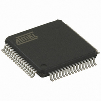
AT89C51CC03U-RDRIM Atmel, AT89C51CC03U-RDRIM Datasheet - Page 37

AT89C51CC03U-RDRIM
Manufacturer Part Number
AT89C51CC03U-RDRIM
Description
IC 8051 MCU FLASH 64K 64VQFP
Manufacturer
Atmel
Series
AT89C CANr
Datasheets
1.AT89C51CC03C-S3RIM.pdf
(198 pages)
2.AT89C51CC03C-S3RIM.pdf
(32 pages)
3.AT89C51CC03C-S3RIM.pdf
(27 pages)
4.AT89C51CC03C-S3RIM.pdf
(184 pages)
Specifications of AT89C51CC03U-RDRIM
Core Processor
8051
Core Size
8-Bit
Speed
40MHz
Connectivity
CAN, SPI, UART/USART
Peripherals
POR, PWM, WDT
Number Of I /o
36
Program Memory Size
64KB (64K x 8)
Program Memory Type
FLASH
Eeprom Size
2K x 8
Ram Size
2.25K x 8
Voltage - Supply (vcc/vdd)
3 V ~ 5.5 V
Data Converters
A/D 8x10b
Oscillator Type
External
Operating Temperature
-40°C ~ 85°C
Package / Case
64-TQFP, 64-VQFP
Lead Free Status / RoHS Status
Contains lead / RoHS non-compliant
Other names
AT89C51CC03URDRTR
Available stocks
Company
Part Number
Manufacturer
Quantity
Price
- AT89C51CC03C-S3RIM PDF datasheet
- AT89C51CC03C-S3RIM PDF datasheet #2
- AT89C51CC03C-S3RIM PDF datasheet #3
- AT89C51CC03C-S3RIM PDF datasheet #4
- Current page: 37 of 198
- Download datasheet (3Mb)
EEPROM Data
Memory
Write Data in the Column
Latches
Programming
Read Data
4182O–CAN–09/08
The 2-Kbyte on-chip EEPROM memory block is located at addresses 0000h to 07FFh of
the XRAM/ERAM memory space and is selected by setting control bits in the EECON
register. A read in the EEPROM memory is done with a MOVX instruction.
A physical write in the EEPROM memory is done in two steps: write data in the column
latches and transfer of all data latches into an EEPROM memory row (programming).
The number of data written on the page may vary from 1 up to 128 Bytes (the page
size). When programming, only the data written in the column latch is programmed and
a ninth bit is used to obtain this feature. This provides the capability to program the
whole memory by Bytes, by page or by a number of Bytes in a page. Indeed, each ninth
bit is set when the writing the corresponding byte in a row and all these ninth bits are
reset after the writing of the complete EEPROM row.
Data is written by byte to the column latches as for an external RAM memory. Out of the
11 address bits of the data pointer, the 4 MSBs are used for page selection (row) and 7
are used for byte selection. Between two EEPROM programming sessions, all the
addresses in the column latches must stay on the same page, meaning that the 4 MSB
must no be changed.
The following procedure is used to write to the column latches:
•
•
•
•
•
•
•
Note:
The EEPROM programming consists of the following actions:
•
•
•
•
Note:
The following procedure is used to read the data stored in the EEPROM memory:
•
•
•
•
•
Save and disable interrupt.
Set bit EEE of EECON register
Load DPTR with the address to write
Store A register with the data to be written
Execute a MOVX @DPTR, A
If needed loop the three last instructions until the end of a 128 Bytes page
Restore interrupt.
writing one or more Bytes of one page in the column latches. Normally, all Bytes
must belong to the same page; if not, the first page address will be latched and the
others discarded.
launching programming by writing the control sequence (50h followed by A0h) to the
EECON register.
EEBUSY flag in EECON is then set by hardware to indicate that programming is in
progress and that the EEPROM segment is not available for reading.
The end of programming is indicated by a hardware clear of the EEBUSY flag.
Save and disable interrupt
Set bit EEE of EECON register
Load DPTR with the address to read
Execute a MOVX A, @DPTR
Restore interrupt
The last page address used when loading the column latch is the one used to select the
page programming address.
The sequence 5xh and Axh must be executed without instructions between then other-
wise the programming is aborted.
AT89C51CC03
37
Related parts for AT89C51CC03U-RDRIM
Image
Part Number
Description
Manufacturer
Datasheet
Request
R

Part Number:
Description:
Manufacturer:
Atmel Corporation
Datasheet:

Part Number:
Description:
At89c51cc03 Enhanced 8-bit Mcu With Can Controller And Flash Memory
Manufacturer:
ATMEL Corporation
Datasheet:

Part Number:
Description:
DEV KIT FOR AVR/AVR32
Manufacturer:
Atmel
Datasheet:

Part Number:
Description:
INTERVAL AND WIPE/WASH WIPER CONTROL IC WITH DELAY
Manufacturer:
ATMEL Corporation
Datasheet:

Part Number:
Description:
Low-Voltage Voice-Switched IC for Hands-Free Operation
Manufacturer:
ATMEL Corporation
Datasheet:

Part Number:
Description:
MONOLITHIC INTEGRATED FEATUREPHONE CIRCUIT
Manufacturer:
ATMEL Corporation
Datasheet:

Part Number:
Description:
AM-FM Receiver IC U4255BM-M
Manufacturer:
ATMEL Corporation
Datasheet:

Part Number:
Description:
Monolithic Integrated Feature Phone Circuit
Manufacturer:
ATMEL Corporation
Datasheet:

Part Number:
Description:
Multistandard Video-IF and Quasi Parallel Sound Processing
Manufacturer:
ATMEL Corporation
Datasheet:

Part Number:
Description:
High-performance EE PLD
Manufacturer:
ATMEL Corporation
Datasheet:

Part Number:
Description:
8-bit Flash Microcontroller
Manufacturer:
ATMEL Corporation
Datasheet:

Part Number:
Description:
2-Wire Serial EEPROM
Manufacturer:
ATMEL Corporation
Datasheet:


