MC10ELT25D ON Semiconductor, MC10ELT25D Datasheet
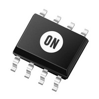
Translation - Voltage Levels -5V Diff ECL to TTL

MC10ELT25D

Manufacturer Part Number
MC10ELT25D
Description
Translation - Voltage Levels -5V Diff ECL to TTL
Manufacturer
ON Semiconductor
Datasheet

Specifications of MC10ELT25D

Logic Type
Translator
Logic Family
ECL
Package / Case
SOIC-8
Translation
ECL to TTL
Propagation Delay Time
4.1 ns
Supply Voltage (max)
- 5.7 V, + 5.5 V
Supply Voltage (min)
- 4.2 V, + 4.5 V
Maximum Operating Temperature
+ 85 C
Minimum Operating Temperature
- 40 C
Mounting Style
SMD/SMT
Lead Free Status / Rohs Status
No RoHS Version Available

Available stocks

Company
Part Number
Manufacturer
Quantity
Price
Part Number:
MC10ELT25D
Manufacturer:
MOTOROLA/摩托罗拉
Quantity:
20 000
Part Number:
MC10ELT25DR2
Manufacturer:
ON/安森美
Quantity:
20 000
Part Number:
MC10ELT25DTG
Manufacturer:
ON Semiconductor
Quantity:
500
MC10ELT25, MC100ELT25
-5 V Differential ECL to TTL
Translator
Description
Because ECL levels are used, a +5 V, −5.2 V (or −4.5 V) and ground
are required. The small outline 8-lead package and the single gate of
the ELT25 makes it ideal for those applications where space,
performance and low power are at a premium.
this device only. For single-ended input conditions, the unused
differential input is connected to V
V
and V
to 0.5 mA. When not used, V
Features
© Semiconductor Components Industries, LLC, 2008
August, 2008 − Rev. 13
BB
The MC10ELT/100ELT25 is a differential ECL to TTL translator.
The V
The 100 Series contains temperature compensation.
V
2.6 ns Typical Propagation Delay
100 MHz F
24 mA TTL Outputs
Flow Through Pinouts
Operating Range: V
Internal Input 50 KW Pulldown Resistors
Q Output will default HIGH with inputs open or < 1.3 V
Pb−Free Packages are Available
EE
may also rebias AC coupled inputs. When used, decouple V
CC
= −4.2 V to −5.7 V with GND = 0 V
BB
via a 0.01 mF capacitor and limit current sourcing or sinking
pin, an internally generated voltage supply, is available to
MAX
CLK
CC
= 4.5 V to 5.5 V with GND = 0 V;
BB
should be left open.
BB
as a switching reference voltage.
1
BB
See detailed ordering and shipping information in the package
dimensions section on page 5 of this data sheet.
CASE 506AA
MN SUFFIX
CASE 948R
DT SUFFIX
CASE 751
D SUFFIX
H
K
5F
2U
M
TSSOP−8
*For additional marking information, refer to
8
(Note: Microdot may be in either location)
SOIC−8
Application Note AND8002/D.
DFN8
8
= MC10
= MC100
= MC10
= MC100
= Date Code
1
ORDERING INFORMATION
1
http://onsemi.com
8
1
8
1
MARKING DIAGRAMS*
ALYWG
1
HT25
A
L
Y
W
G
Publication Order Number:
HLT25
ALYW
G
G
4
= Assembly Location
= Wafer Lot
= Year
= Work Week
= Pb−Free Package
8
1
MC10ELT25/D
8
1
KLT25
ALYW
1
ALYWG
KT25
G
G
4

Related parts for MC10ELT25D

MC10ELT25D Summary of contents

Page 1

MC10ELT25, MC100ELT25 -5 V Differential ECL to TTL Translator Description The MC10ELT/100ELT25 is a differential ECL to TTL translator. Because ECL levels are used −5.2 V (or −4.5 V) and ground are required. The small outline 8-lead package ...

Page 2

TTL D 2 ECL Figure 1. 8−Lead Pinout (Top View) and Logic Diagram Table 2. ATTRIBUTES Internal Input Pulldown Resistor Internal Input Pullup Resistor ESD Protection Moisture Sensitivity, Indefinite Time Out of ...

Page 3

Table 4. 10ELT SERIES NECL INPUT DC CHARACTERISTICS Symbol Characteristic V Input HIGH Voltage (Single−Ended) (Note Input LOW Voltage (Single−Ended) (Note Output Voltage Reference BB V Input HIGH Voltage Common Mode Range IHCMR (Differential) ...

Page 4

Table 7. AC CHARACTERISTICS V Symbol Characteristic f Maximum Toggle Frequency max t Propagation Delay @ 1.5 V PLH t Propagation Delay @ 1.5 V PHL t Random Clock Jitter (RMS) JITTER t Output Rise/Fall Times QTTL r t 10% ...

Page 5

... ORDERING INFORMATION Device MC10ELT25D MC10ELT25DG MC10ELT25DR2 MC10ELT25DR2G MC10ELT25DT MC10ELT25DTG MC10ELT25DTR2 MC10ELT25DTR2G MC10ELT25MNR4 MC10ELT25MNR4G MC100ELT25D MC100ELT25DG MC100ELT25DR2 MC100ELT25DR2G MC100ELT25DT MC100ELT25DTG MC100ELT25DTR2 MC100ELT25DTR2G MC100ELT25MNR4 MC100ELT25MNR4G †For information on tape and reel specifications, including part orientation and tape sizes, please refer to our Tape and Reel Packaging Specifications Brochure, BRD8011/D ...

Page 6

... G C SEATING PLANE −Z− 0.25 (0.010 *For additional information on our Pb−Free strategy and soldering details, please download the ON Semiconductor Soldering and Mounting Techniques Reference Manual, SOLDERRM/D. PACKAGE DIMENSIONS SOIC−8 NB CASE 751−07 ISSUE 0.10 (0.004 SOLDERING FOOTPRINT* 1 ...

Page 7

K 8x REF 0.10 (0.004) 0.15 (0.006 L −U− PIN 1 IDENT 0.15 (0.006 −V− C 0.10 (0.004) D −T− G SEATING PLANE PACKAGE DIMENSIONS TSSOP−8 ...

Page 8

... Opportunity/Affirmative Action Employer. This literature is subject to all applicable copyright laws and is not for resale in any manner. PUBLICATION ORDERING INFORMATION LITERATURE FULFILLMENT: Literature Distribution Center for ON Semiconductor P.O. Box 5163, Denver, Colorado 80217 USA Phone: 303−675−2175 or 800−344−3860 Toll Free USA/Canada Fax: 303− ...

Related keywords