STEVAL-CCA003V1 STMicroelectronics, STEVAL-CCA003V1 Datasheet
STEVAL-CCA003V1
Specifications of STEVAL-CCA003V1
STEVAL-CCA003V1
Available stocks


Related parts for STEVAL-CCA003V1


STEVAL-CCA003V1 Summary of contents
Page 1
Operating from V =2.2V to 5.5V CC ■ 1W output power per channel @ V THD+N=1%, RL=8Ω ■ 10nA standby current ■ 62dB PSRR @ 217Hz with grounded inputs ■ High SNR: 100dB(A) typ. ■ Near-zero pop & click ...
Page 2
TS4984 1 Typical Application Figure 1 shows a schematic view of a typical audio amplification application using the TS4984. describes the components used in this typical application. Figure 1: Typical application schematic Input L Cin-L GND 100n VCC 1 2 ...
Page 3
Absolute maximum ratings and operating conditions 2 Absolute maximum ratings and operating conditions Table 2: Key parameters and their absolute maximum ratings Symbol 1 V Supply voltage Input Voltage i T Operating Free Air Temperature Range oper ...
Page 4
TS4984 3 Electrical characteristics Table 4: Electrical characteristics for V specified) Symbol Supply Current input signal, no load 1 Standby Current I STANDBY No input signal, Vstdby = G Output Offset Voltage Voo No input signal, RL ...
Page 5
Electrical characteristics Table 5: Electrical characteristics for V specified) Symbol Supply Current input signal, no load 1 Standby Current I STANDBY No input signal, Vstdby = G Output Offset Voltage Voo No input signal ...
Page 6
TS4984 Table 6: Electrical characteristics for V specified) Symbol Supply Current input signal, no load 1 Standby Current I STANDBY No input signal, Vstdby = G Output Offset Voltage Voo No input signal Ω ...
Page 7
Electrical characteristics Figure 2: Open loop frequency response 60 Gain 40 Phase 20 0 -20 Vcc = 5V - Ω Tamb = 25 ° C -60 0 100 Frequency (kHz) Figure 3: Open loop frequency ...
Page 8
TS4984 Figure 8: Power supply rejection ratio (PSRR) vs. frequency 0 Vripple = 200mVpp - Input = Grounded - Cin = 1 µ F Vcc : RL >= 4 Ω 2.2V Tamb = 25 ° ...
Page 9
Electrical characteristics Figure 14: Power supply rejection ratio (PSRR) vs. DC output voltage 0 Vcc = 5V -10 Vripple = 200mVpp Ω µ Tamb = 25 ° C -30 ...
Page 10
TS4984 Figure 20: Power supply rejection ratio (PSRR) vs. DC output voltage 0 Vcc = 2.6V Vripple = 200mVpp - Ω µ Tamb = 25 ° C -30 -40 ...
Page 11
Electrical characteristics Figure 26: Output power vs. power supply voltage 1 Ω 0 1kHz THD+N=10% 0.8 BW < 125kHz Tamb = 25 ° C 0.7 0.6 0.5 0.4 0.3 0.2 0.1 0.0 2.5 3.0 3.5 ...
Page 12
TS4984 Figure 32: Power dissipation vs. output power 1.2 Vcc=3.3V F=1kHz 1.0 THD+N<1% 0.8 RL=4 Ω 0.6 RL=8 Ω 0.4 0.2 RL=16 Ω 0.0 0.0 0.1 0.2 0.3 Output Power (W) Figure 33: Power dissipation vs. output power 0.7 Vcc=2.6V ...
Page 13
Electrical characteristics Figure 38: Current consumption vs. standby voltage at Vcc=3.3V Figure 39: Current consumption vs. standby voltage at Vcc=2.6V Figure 40: Current consumption vs. standby voltage at Vcc=2.2V Figure 41: THD+N vs. output power Ω ...
Page 14
TS4984 Figure 44: THD+N vs. output power Ω Vcc = 2. 1kHz Vcc = 2. µ < 125kHz Vcc = 3.3V Tamb = 25°C Vcc ...
Page 15
Electrical characteristics Figure 50: THD+N vs. frequency RL=4 Ω Av µ F 0.1 Vcc=5V, Po=1W Bw < 125kHz Tamb = 25 ° C Vcc=2.2V, Po=40mW 0.01 20 100 1000 Frequency (Hz) Figure 51: THD+N vs. frequency RL=8 ...
Page 16
TS4984 Figure 56: SIgnal to noise ratio vs. power supply with A weighted filter 95 90 RL=8 Ω 85 RL=4 Ω 80 2.5 3.0 3.5 Power Supply Voltage (V) Figure 57: Crosstalk vs. frequency 0 Vcc = ...
Page 17
Electrical characteristics Figure 62: Output noise voltage, device in standby 3.00 2.75 2.50 2.25 Unweighted Filter 2.00 1.75 1.50 1.25 1.00 Vcc = 2. 0. µ Ω 0.25 Tamb = ...
Page 18
TS4984 4 Application Information The TS4984 integrates two monolithic power amplifiers with a BTL (Bridge Tied Load) output type (explained in more detail in referred to. Referring to the schematic IN ...
Page 19
Application Information 4.2 Gain in typical application schematic The typical application schematic In the flat region (no C effect), the output voltage of the first stage is: in For the second stage out2 The differential output voltage ...
Page 20
TS4984 The following graph (Figure 65) shows an example of C Figure 65: Frequency response gain versus C 4.4 Power dissipation and efficiency Hypotheses: Voltage and current in the load are sinusoidal (V Supply voltage is a pure DC source ...
Page 21
Application Information Then, the power dissipated by each amplifier is: and the maximum value is obtained when: and its value is: Note: This maximum value is only depending on power supply voltage and load values. The efficiency, η, is the ...
Page 22
TS4984 4.5 Decoupling the circuit Two capacitors are needed to correctly bypass the TS4984. A power supply bypass capacitor C bias voltage bypass capacitor C C has particular influence on the THD+N in the high frequency region (above 7 kHz) ...
Page 23
Application Information 4.7 Shutdown time When the standby command is set, the time required to put the two output stages in high impedance and the internal circuitry in shutdown mode is a few microseconds. Note: In shutdown mode, Bypass pin ...
Page 24
TS4984 4.9 Application example: Differential-input BTL power stereo amplifier The schematic in Figure 69 shows how to design the TS4984 to work in differential-input mode. For this discussion, only the left-channel amplifier will be referred to. Let ...
Page 25
Application Information The value of the input capacitor C frequency required (where F L Note: This formula is true only if π times lower than ...
Page 26
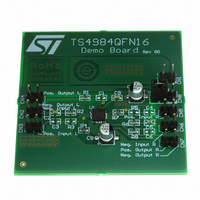
TS4984 4.10 Demoboard A demoboard for the TS4984 is available. For more information about this demoboard, please refer to Application Note AN2049, which can be found on www.st.com. Figure 70 shows the schematic of the demoboard. component locations, top layer ...
Page 27
Application Information Figure 71: Components location Figure 73: Bottom layer Figure 72: Top layer TS4984 27/29 ...
Page 28
TS4984 5 Package Mechanical Data 5.1 Dimensions of QFN16 package * The Exposed Pad is connected to Ground. * The Exposed Pad is connected to Ground. 5.2 Footprint recommended data 28/ ...
Page 29
... STMicroelectronics. Specifications mentioned in this publication are subject by implication or otherwise under any patent or patent rights of STMicroelectronics. Specifications mentioned in this publication are subject to change without notice. This publication supersedes and replaces all information previously supplied. STMicroelectronics products are not to change without notice ...