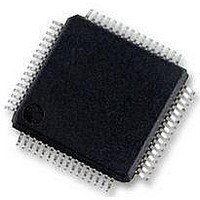
STM32F405RGT6 STMicroelectronics, STM32F405RGT6 Datasheet - Page 100

STM32F405RGT6
Manufacturer Part Number
STM32F405RGT6
Description
Microcontrollers (MCU) ARM M4 1024 FLASH 168 Mhz 192kB SRAM
Manufacturer
STMicroelectronics
Datasheet
1.STM32F407ZGT6.pdf
(167 pages)
Specifications of STM32F405RGT6
Core
ARM Cortex M4
Processor Series
STM32F4
Data Bus Width
32 bit
Maximum Clock Frequency
168 MHz
Program Memory Size
1024 KB
Data Ram Size
192 KB
On-chip Adc
Yes
Number Of Programmable I/os
51
Number Of Timers
10
Operating Supply Voltage
1.7 V to 3.6 V
Package / Case
LQFP-64
Mounting Style
SMD/SMT
A/d Bit Size
12 bit
A/d Channels Available
16
Interface Type
CAN, I2C, I2S, SPI, UART
Program Memory Type
Flash
Lead Free Status / Rohs Status
Details
Available stocks
Company
Part Number
Manufacturer
Quantity
Price
Company:
Part Number:
STM32F405RGT6
Manufacturer:
ON
Quantity:
1 001
Company:
Part Number:
STM32F405RGT6
Manufacturer:
STMicroelectronics
Quantity:
10 000
Part Number:
STM32F405RGT6
Manufacturer:
ST
Quantity:
20 000
Electrical characteristics
100/167
All I/Os are CMOS and TTL compliant (no software configuration required). Their
characteristics cover more than the strict CMOS-technology or TTL parameters.
Output driving current
The GPIOs (general purpose input/outputs) can sink or source up to ±8 mA, and sink or
source ±20 mA (with a relaxed V
In the user application, the number of I/O pins which can drive current must be limited to
respect the absolute maximum rating specified in
●
●
Output voltage levels
Unless otherwise specified, the parameters given in
performed under ambient temperature and V
Table
Table 45.
1. PC13, PC14, PC15 and PI8 are supplied through the power switch. Since the switch only sinks a limited
2. The I
3. The I
4. Based on characterization data, not tested in production.
V
V
Symbol
V
V
V
V
V
V
OH
OH
OL
OL
OH
OL
OH
amount of current (3 mA), the use of GPIOs PC13 to PC15 and PI8 in output mode is limited: the speed
should not exceed 2 MHz with a maximum load of 30 pF and these I/Os must not be used as a current
source (e.g. to drive an LED).
and the sum of I
Table 9
OL
(2)(4)
(2)(4)
(3)(4)
(3)(4)
The sum of the currents sourced by all the I/Os on V
consumption of the MCU sourced on V
I
The sum of the currents sunk by all the I/Os on V
consumption of the MCU sunk on V
I
VDD
VSS
(2)
(3)
(2)
(3)
11. All I/Os are CMOS and TTL compliant.
IO
IO
current sunk by the device must always respect the absolute maximum rating specified in
current sourced by the device must always respect the absolute maximum rating specified in
(see
and the sum of I
(see
Output low level voltage for an I/O pin
when 8 pins are sunk at same time
Output high level voltage for an I/O pin
when 8 pins are sourced at same time
Output low level voltage for an I/O pin
when 8 pins are sunk at same time
Output high level voltage for an I/O pin
when 8 pins are sourced at same time
Output low level voltage for an I/O pin
when 8 pins are sunk at same time
Output high level voltage for an I/O pin
when 8 pins are sourced at same time
Output low level voltage for an I/O pin
when 8 pins are sunk at same time
Output high level voltage for an I/O pin
when 8 pins are sourced at same time
Output voltage characteristics
Table
Table
IO
(I/O ports and control pins) must not exceed I
9).
9).
IO
Parameter
(I/O ports and control pins) must not exceed I
Doc ID 022152 Rev 2
OL
/V
OH
).
SS
DD,
cannot exceed the absolute maximum rating
DD
(1)
cannot exceed the absolute maximum rating
supply voltage conditions summarized in
2.7 V < V
2.7 V < V
2.7 V < V
2 V < V
Section
I
Conditions
I
IO
I
CMOS port
I
Table 45
IO
IO
IO
TTL port
SS
= +20 mA
= +8 mA
= +6 mA
VSS
=+ 8mA
DD
DD
DD
DD
plus the maximum Run
DD,
.
5.2. In particular:
< 2.7 V
< 3.6 V
< 3.6 V
< 3.6 V
STM32F405xx, STM32F407xx
plus the maximum Run
VDD
are derived from tests
.
V
V
V
DD
DD
DD
Min
2.4
-
-
-
-
–0.4
–1.3
–0.4
Max
0.4
0.4
1.3
0.4
-
-
-
-
Table 9
Unit
V
V
V
V


