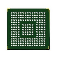
STM32F407IGH6 STMicroelectronics, STM32F407IGH6 Datasheet - Page 125

STM32F407IGH6
Manufacturer Part Number
STM32F407IGH6
Description
Microcontrollers (MCU) ARM M4 1024 FLASH 168 Mhz 192kB SRAM
Manufacturer
STMicroelectronics
Datasheet
1.STM32F407ZGT6.pdf
(167 pages)
Specifications of STM32F407IGH6
Core
ARM Cortex M4
Processor Series
STM32F4
Data Bus Width
32 bit
Maximum Clock Frequency
168 MHz
Program Memory Size
1024 KB
Data Ram Size
192 KB
On-chip Adc
Yes
Number Of Programmable I/os
140
Number Of Timers
10
Operating Supply Voltage
1.7 V to 3.6 V
Package / Case
UFBGA-176
Mounting Style
SMD/SMT
A/d Bit Size
12 bit
A/d Channels Available
24
Interface Type
CAN, I2C, I2S, SPI, UART
Program Memory Type
Flash
Lead Free Status / Rohs Status
Details
Available stocks
Company
Part Number
Manufacturer
Quantity
Price
Company:
Part Number:
STM32F407IGH6
Manufacturer:
STMicroelectronics
Quantity:
1
Company:
Part Number:
STM32F407IGH6
Manufacturer:
STMicroelectronics
Quantity:
10 000
Part Number:
STM32F407IGH6
Manufacturer:
ST
Quantity:
20 000
STM32F405xx, STM32F407xx
Table 70.
1. If an inverted reset signal is applied to PDR_ON, this value can be lowered to 1.7 V when the device operates in a reduced
2. Guaranteed by design, not tested in production.
3. Guaranteed by characterization, not tested in production.
INL
Offset
Gain
error
t
THD
Update
rate
t
PSRR+
SETTLING
WAKEUP
Symbol
temperature range (0 to 70 °C).
(3)
(2)
(3)
(3)
(3)
(2)
(3)
(3)
Integral non linearity
(difference between
measured value at Code i
and the value at Code i on a
line drawn between Code 0
and last Code 1023)
Offset error
(difference between
measured value at Code
(0x800) and the ideal value =
V
Gain error
Settling time (full scale: for a
10-bit input code transition
between the lowest and the
highest input codes when
DAC_OUT reaches final
value ±4LSB
Total Harmonic Distortion
Buffer ON
Max frequency for a correct
DAC_OUT change when
small variation in the input
code (from code i to i+1LSB)
Wakeup time from off state
(Setting the ENx bit in the
DAC Control register)
Power supply rejection ratio
(to V
measurement)
DAC characteristics (continued)
REF+
DDA
/2)
) (static DC
Parameter
Min
-
-
-
-
-
-
-
-
-
-
-
Doc ID 022152 Rev 2
Typ
–67
6.5
3
-
-
-
-
-
-
-
-
Max
±0.5
±10
±12
–40
±1
±4
±3
10
6
1
-
MS/s
Unit
LSB
LSB
LSB
LSB
mV
dB
dB
µs
µs
%
Given for the DAC in 10-bit
configuration.
Given for the DAC in 12-bit
configuration.
Given for the DAC in 12-bit
configuration
Given for the DAC in 10-bit at
V
Given for the DAC in 12-bit at
V
Given for the DAC in 12-bit
configuration
C
R
C
R
C
R
C
input code between lowest and
highest possible ones.
No R
REF+
REF+
LOAD
LOAD
LOAD
LOAD
LOAD
LOAD
LOAD
LOAD
Electrical characteristics
= 3.6 V
= 3.6 V
≤ 50 pF,
≥ 5 kΩ
≤ 50 pF,
≥ 5 kΩ
≤ 50 pF,
≥ 5 kΩ
≤ 50 pF, R
, C
Comments
LOAD
LOAD
= 50 pF
≥ 5 kΩ
125/167


