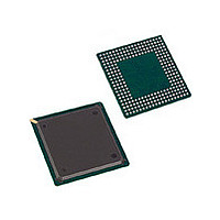
MPC850DSLZQ50BU Freescale Semiconductor, MPC850DSLZQ50BU Datasheet - Page 55

MPC850DSLZQ50BU
Manufacturer Part Number
MPC850DSLZQ50BU
Description
IC MPU PWRQUICC 50MHZ 256-PBGA
Manufacturer
Freescale Semiconductor
Specifications of MPC850DSLZQ50BU
Processor Type
MPC8xx PowerQUICC 32-Bit
Speed
50MHz
Voltage
3.3V
Mounting Type
Surface Mount
Package / Case
256-PBGA
Family Name
MPC8xx
Device Core
PowerQUICC
Device Core Size
32b
Frequency (max)
50MHz
Instruction Set Architecture
RISC
Supply Voltage 1 (typ)
3.3V
Operating Supply Voltage (max)
3.465V
Operating Supply Voltage (min)
3.135V
Operating Temp Range
0C to 95C
Operating Temperature Classification
Commercial
Mounting
Surface Mount
Pin Count
256
Package Type
BGA
Lead Free Status / RoHS Status
Contains lead / RoHS non-compliant
Features
-
Lead Free Status / Rohs Status
Not Compliant
Available stocks
Company
Part Number
Manufacturer
Quantity
Price
Company:
Part Number:
MPC850DSLZQ50BU
Manufacturer:
FREESCAL
Quantity:
364
Company:
Part Number:
MPC850DSLZQ50BU
Manufacturer:
Freescale Semiconductor
Quantity:
10 000
Part Number:
MPC850DSLZQ50BU
Manufacturer:
FREESCALE
Quantity:
20 000
8.6
Table 8-18 provides the NMSI external clock timing.
Table 8-19 provides the NMSI internal clock timing.
MOTOROLA
1
2
1
2
The ratios SyncCLK/RCLKx and SyncCLK/TCLKx must be greater than or equal to 2.25/1.
Also applies to CD and CTS hold time when they are used as an external sync signal.
Num
Num
The ratios SyncCLK/RCLKx and SyncCLK/TCLK1x must be greater or equal to 3/1.
Also applies to CD and CTS hold time when they are used as an external sync signals.
100
102
103
104
105
106
107
108
100
101
102
103
104
105
106
107
108
SCC in NMSI Mode Electrical Specifications
RCLKx and TCLKx frequency
RCLKx and TCLKx rise/fall time
TXDx active delay (from TCLKx falling edge)
RTSx active/inactive delay (from TCLKx falling edge)
CTSx setup time to TCLKx rising edge
RXDx setup time to RCLKx rising edge
RXDx hold time from RCLKx rising edge
CDx setup time to RCLKx rising edge
RCLKx and TCLKx frequency
table)
RCLKx and TCLKx width low
RCLKx and TCLKx rise/fall time
TXDx active delay (from TCLKx falling edge)
RTSx active/inactive delay (from TCLKx falling edge)
CTSx setup time to TCLKx rising edge
RXDx setup time to RCLKx rising edge
RXDx hold time from RCLKx rising edge
CDx setup time to RCLKx rising edge
Table 8-18. NMSI External Clock Timing
Freescale Semiconductor, Inc.
Table 8-19. NMSI Internal Clock Timing
MPC850 (Rev. A/B/C) Hardware Specifications
For More Information On This Product,
Characteristic
Characteristic
1
(x = 2, 3 for all specs in this table)
Go to: www.freescale.com
1
(x = 2, 3 for all specs in this
2
2
SCC in NMSI Mode Electrical Specifications
1/SYNCCLK +5
1/SYNCCLK
40.00
40.00
40.00
0.00
0.00
0.00
0.00
Min
—
All Frequencies
All Frequencies
0.00
0.00
5.00
5.00
5.00
5.00
Min
—
SYNCCLK/3
30.00
30.00
Max
—
—
—
—
—
15.00 ns
50.00 ns
50.00 ns
Max
—
—
—
—
—
—
ns
ns
ns
ns
ns
ns
MHz
Unit
ns
ns
ns
ns
ns
ns
ns
Unit
55


