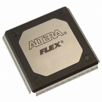
EPF10K50RI240-4 Altera, EPF10K50RI240-4 Datasheet - Page 37

EPF10K50RI240-4
Manufacturer Part Number
EPF10K50RI240-4
Description
IC FLEX 10K FPGA 50K 240-RQFP
Manufacturer
Altera
Series
FLEX-10K®r
Datasheet
1.EPF10K10ATC100-3.pdf
(128 pages)
Specifications of EPF10K50RI240-4
Number Of Logic Elements/cells
2880
Number Of Labs/clbs
360
Total Ram Bits
20480
Number Of I /o
189
Number Of Gates
116000
Voltage - Supply
4.5 V ~ 5.5 V
Mounting Type
Surface Mount
Operating Temperature
-40°C ~ 100°C
Package / Case
240-RQFP
Lead Free Status / RoHS Status
Contains lead / RoHS non-compliant
Other names
544-2240
Available stocks
Company
Part Number
Manufacturer
Quantity
Price
Company:
Part Number:
EPF10K50RI240-4
Manufacturer:
ALTERA
Quantity:
12 388
Company:
Part Number:
EPF10K50RI240-4
Manufacturer:
ALTERA30
Quantity:
50
Part Number:
EPF10K50RI240-4
Manufacturer:
ALTERA/阿尔特拉
Quantity:
20 000
Company:
Part Number:
EPF10K50RI240-4N
Manufacturer:
BCD
Quantity:
91 500
Part Number:
EPF10K50RI240-4N
Manufacturer:
ALTERA/阿尔特拉
Quantity:
20 000
Altera Corporation
ClockLock &
ClockBoost
Features
To support high-speed designs, selected FLEX 10K devices offer optional
ClockLock and ClockBoost circuitry containing a phase-locked loop (PLL)
that is used to increase design speed and reduce resource usage. The
ClockLock circuitry uses a synchronizing PLL that reduces the clock delay
and skew within a device. This reduction minimizes clock-to-output and
setup times while maintaining zero hold times. The ClockBoost circuitry,
which provides a clock multiplier, allows the designer to enhance device
area efficiency by sharing resources within the device. The ClockBoost
feature allows the designer to distribute a low-speed clock and multiply
that clock on-device. Combined, the ClockLock and ClockBoost features
provide significant improvements in system performance and
bandwidth.
The ClockLock and ClockBoost features in FLEX 10K devices are enabled
through the Altera software. External devices are not required to use these
features. The output of the ClockLock and ClockBoost circuits is not
available at any of the device pins.
The ClockLock and ClockBoost circuitry locks onto the rising edge of the
incoming clock. The circuit output can only drive the clock inputs of
registers; the generated clock cannot be gated or inverted.
The dedicated clock pin (GCLK1) supplies the clock to the ClockLock and
ClockBoost circuitry. When the dedicated clock pin is driving the
ClockLock or ClockBoost circuitry, it cannot drive elsewhere in the device.
In designs that require both a multiplied and non-multiplied clock, the
clock trace on the board can be connected to GCLK1. With the Altera
software, GCLK1 can feed both the ClockLock and ClockBoost circuitry in
the FLEX 10K device. However, when both circuits are used, the other
clock pin (GCLK0) cannot be used.
how to enable both the ClockLock and ClockBoost circuits in the Altera
software. The example shown is a schematic, but a similar approach
applies for designs created in AHDL, VHDL, and Verilog HDL. When the
ClockLock and ClockBoost circuits are used simultaneously, the input
frequency parameter must be the same for both circuits. In
input frequency must meet the requirements specified when the
ClockBoost multiplication factor is two.
FLEX 10K Embedded Programmable Logic Device Family Data Sheet
Figure 17
shows a block diagram of
Figure
17, the
37


