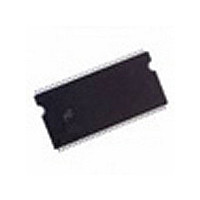
MT46V32M16D2TH-7L Micron Technology Inc, MT46V32M16D2TH-7L Datasheet - Page 14

MT46V32M16D2TH-7L
Manufacturer Part Number
MT46V32M16D2TH-7L
Description
Manufacturer
Micron Technology Inc
Type
DDR SDRAMr
Datasheet
1.MT46V32M16D2TH-7L.pdf
(70 pages)
Specifications of MT46V32M16D2TH-7L
Organization
32Mx16
Density
512Mb
Address Bus
15b
Access Time (max)
750ps
Maximum Clock Rate
266MHz
Operating Supply Voltage (typ)
2.5V
Package Type
TSOP
Operating Temp Range
0C to 70C
Operating Supply Voltage (max)
2.7V
Operating Supply Voltage (min)
2.3V
Pin Count
66
Mounting
Surface Mount
Operating Temperature Classification
Commercial
Lead Free Status / Rohs Status
Not Compliant
DESELECT
commands from being executed by the DDR SDRAM.
The DDR SDRAM is effectively deselected. Operations
already in progress are not affected.
NO OPERATION (NOP)
instruct the selected DDR SDRAM to perform a NOP
(CS# LOW). This prevents unwanted commands from
being registered during idle or wait states. Operations
already in progress are not affected.
LOAD MODE REGISTER
See mode register descriptions in the Register Defini-
tion section. The LOAD MODE REGISTER command
can only be issued when all banks are idle, and a
subsequent executable command cannot be issued until
t
ACTIVE
a row in a particular bank for a subsequent access. The
value on the BA0, BA1 inputs selects the bank, and the
address provided on inputs A0–A12 selects the row.
This row remains active (or open) for accesses until a
PRECHARGE command is issued to that bank.
A PRECHARGE command must be issued before open-
ing a different row in the same bank.
READ
access to an active row. The value on the BA0, BA1
inputs selects the bank, and the address provided on
inputs A0–Ai (where i = 9 for x16; 9, 11 for x8; or 9, 11,
and 12 for x4) selects the starting column location. The
value on input A10 determines whether or not auto
precharge is used. If auto precharge is selected, the row
being accessed will be precharged at the end of the
READ burst; if auto precharge is not selected, the row
will remain open for subsequent accesses.
WRITE
access to an active row. The value on the BA0, BA1
inputs selects the bank, and the address provided on
inputs A0–Ai (where i = 9 for x16; 9 and 11 for x8; or 9,
11, and 12 for x4) selects the starting column location.
The value on input A10 determines whether or not auto
precharge is used. If auto precharge is selected, the row
being accessed will be precharged at the end of the
WRITE burst; if auto precharge is not selected, the row
will remain open for subsequent accesses. Input data
512Mb: x4, x8, x16 DDR SDRAM
512Mx4x8x16DDR_A.p65 – Rev. A; Pub 10/00
MRD is met.
The DESELECT function (CS# HIGH) prevents new
The NO OPERATION (NOP) command is used to
The mode registers are loaded via inputs A0–A12.
The ACTIVE command is used to open (or activate)
The READ command is used to initiate a burst read
The WRITE command is used to initiate a burst write
14
appearing on the DQs is written to the memory array
subject to the DM input logic level appearing coincident
with the data. If a given DM signal is registered LOW, the
corresponding data will be written to memory; if the
DM signal is registered HIGH, the corresponding data
inputs will be ignored, and a WRITE will not be executed
to that byte/column location.
PRECHARGE
open row in a particular bank or the open row in all
banks. The bank(s) will be available for a subsequent row
access a specified time (
mand is issued. Input A10 determines whether one or all
banks are to be precharged, and in the case where only
one bank is to be precharged, inputs BA0, BA1 select the
bank. Otherwise BA0, BA1 are treated as “Don’t Care.”
Once a bank has been precharged, it is in the idle state
and must be activated prior to any READ or WRITE
commands being issued to that bank. A PRECHARGE
command will be treated as a NOP if there is no open
row in that bank (idle state), or if the previously open
row is already in the process of precharging.
AUTO PRECHARGE
same individual-bank precharge function described
above, but without requiring an explicit command.
This is accomplished by using A10 to enable auto
precharge in conjunction with a specific READ or
WRITE command. A precharge of the bank/row that is
addressed with the READ or WRITE command is auto-
matically performed upon completion of the READ or
WRITE burst. Auto precharge is nonpersistent in that it
is either enabled or disabled for each individual READ
or WRITE command.
ated at the earliest valid stage within a burst. This
“earliest valid stage” is determined as if an explicit
PRECHARGE command was issued at the earliest pos-
sible time, without violating
for each burst type in the Operation section of this data
sheet. The user must not issue another command to the
same bank until the precharge time (
BURST TERMINATE
cate READ bursts (with auto precharge disabled). The
most recently registered READ command prior to the
BURST TERMINATE command will be truncated, as
shown in the Operation section of this data sheet. The
open page which the READ burst was terminated from
remains open.
The PRECHARGE command is used to deactivate the
Auto precharge is a feature which performs the
Auto precharge ensures that the precharge is initi-
The BURST TERMINATE command is used to trun-
Micron Technology, Inc., reserves the right to change products or specifications without notice.
512Mb: x4, x8, x16
t
RP) after the PRECHARGE com-
t
RAS (MIN), as described
DDR SDRAM
t
RP) is completed.
©2000, Micron Technology, Inc.
ADVANCE


