NTHD3102CT1G ON Semiconductor, NTHD3102CT1G Datasheet - Page 2
NTHD3102CT1G
Manufacturer Part Number
NTHD3102CT1G
Description
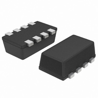
MOSFET N/P-CH COMPL 20V CHIPFET
Manufacturer
ON Semiconductor
Datasheet
1.NTHD3102CT1G.pdf
(11 pages)
Specifications of NTHD3102CT1G
Fet Type
N and P-Channel
Fet Feature
Logic Level Gate
Rds On (max) @ Id, Vgs
45 mOhm @ 4.4A, 4.5V
Drain To Source Voltage (vdss)
20V
Current - Continuous Drain (id) @ 25° C
4A, 3.1A
Vgs(th) (max) @ Id
1.2V @ 250µA
Gate Charge (qg) @ Vgs
7.9nC @ 4.5V
Input Capacitance (ciss) @ Vds
510pF @ 10V
Power - Max
1.1W
Mounting Type
Surface Mount
Package / Case
8-ChipFET™
Lead Free Status / RoHS Status
Lead free / RoHS Compliant
Other names
NTHD3102CT1G
NTHD3102CT1GOSTR
NTHD3102CT1GOSTR
Available stocks
Company
Part Number
Manufacturer
Quantity
Price

Part Number:
NTHD3102CT1G
Manufacturer:
ON/安森美
Quantity:
20 000


Stresses exceeding Maximum Ratings may damage the device. Maximum Ratings are stress ratings only. Functional operation above the
Recommended Operating Conditions is not implied. Extended exposure to stresses above the Recommended Operating Conditions may affect
device reliability.
2. Surface−mounted on FR4 board using 1 in sq pad size (Cu area = 1.127 in sq [1 oz] including traces).
3. Surface−mounted on FR4 board using the minimum recommended pad size (Cu area = TBD in sq).
4. Switching characteristics are independent of operating junction temperatures.
MAXIMUM RATINGS
THERMAL RESISTANCE RATINGS
ELECTRICAL CHARACTERISTICS
OFF CHARACTERISTICS
N−Channel
Continuous Drain Current (Note 3)
P−Channel
Continuous Drain Current (Note 3)
Power Dissipation (Note 3)
Pulsed Drain Current
Operating Junction and Storage Temperature
Source Current (Body Diode)
Lead Temperature for Soldering Purposes (1/8″ from case for 10 seconds)
Junction−to−Ambient − Steady State (Note 2)
Junction−to−Ambient − t ≤ 5 s (Note 2)
Junction−to−Ambient − Steady State (Note 3)
Drain−to−Source Breakdown Voltage
(Note 4)
Drain−to−Source Breakdown Voltage
Temperature Coefficient
Zero Gate Voltage Drain Current
Gate−to−Source Leakage Current
Parameter
(continued) (T
J
V
= 25°C unless otherwise noted)
(T
V
(BR)DSS
Symbol
(BR)DSS
J
Parameter
Parameter
I
I
GSS
DSS
= 25°C unless otherwise noted)
/T
J
N/P
N
P
N
P
N
P
N
P
N
P
http://onsemi.com
NTHD3102C
V
V
V
V
GS
GS
GS
GS
2
= 0 V, V
= 0 V, V
= 0 V, V
= 0 V, V
V
V
V
GS
DS
DS
Steady
Steady
N−Ch
P−Ch
State
State
= 0 V
Test Conditions
DS
DS
= 0 V, V
= 0 V, V
DS
DS
= −16 V
= −16 V
= 16 V
= 16 V
GS
GS
T
T
T
T
T
tp = 10 ms
= ±8.0 V
= ±8.0 V
A
A
A
A
A
= 25°C
= 85°C
= 25°C
= 85°C
= 25°C
I
I
D
D
T
T
= −250 mA
J
J
= 250 mA
= 25 °C
= 85 °C
T
Symbol
Symbol
J
R
, T
I
P
DM
T
I
I
I
qJA
D
D
S
Min
−20
D
L
STG
20
20.2
16.2
Typ
−55 to 150
Value
12.6
Max
260
110
195
3.0
2.2
2.3
1.7
0.6
1.7
16
60
±100
±100
Max
−1.0
−5.0
1.0
5.0
mV/°C
°C/W
Unit
Unit
Unit
°C
°C
W
mA
nA
A
A
A
A
V
Related parts for NTHD3102CT1G
Image
Part Number
Description
Manufacturer
Datasheet
Request
R

Part Number:
Description:
ON Semiconductor [VOLTAGE REGULATOR]
Manufacturer:
ON Semiconductor
Datasheet:
Part Number:
Description:
357-036-542-201 CARDEDGE 36POS DL .156 BLK LOPRO
Manufacturer:
ON Semiconductor
Datasheet:
Part Number:
Description:
357-036-542-201 CARDEDGE 36POS DL .156 BLK LOPRO
Manufacturer:
ON Semiconductor
Datasheet:
Part Number:
Description:
357-036-542-201 CARDEDGE 36POS DL .156 BLK LOPRO
Manufacturer:
ON Semiconductor
Datasheet:
Part Number:
Description:
357-036-542-201 CARDEDGE 36POS DL .156 BLK LOPRO
Manufacturer:
ON Semiconductor
Datasheet:
Part Number:
Description:
357-036-542-201 CARDEDGE 36POS DL .156 BLK LOPRO
Manufacturer:
ON Semiconductor
Datasheet:
Part Number:
Description:
357-036-542-201 CARDEDGE 36POS DL .156 BLK LOPRO
Manufacturer:
ON Semiconductor
Datasheet:
Part Number:
Description:
357-036-542-201 CARDEDGE 36POS DL .156 BLK LOPRO
Manufacturer:
ON Semiconductor
Datasheet:
Part Number:
Description:
357-036-542-201 CARDEDGE 36POS DL .156 BLK LOPRO
Manufacturer:
ON Semiconductor
Datasheet:
Part Number:
Description:
357-036-542-201 CARDEDGE 36POS DL .156 BLK LOPRO
Manufacturer:
ON Semiconductor
Datasheet:
Part Number:
Description:
357-036-542-201 CARDEDGE 36POS DL .156 BLK LOPRO
Manufacturer:
ON Semiconductor
Datasheet:
Part Number:
Description:
Manufacturer:
ON Semiconductor
Datasheet:
Part Number:
Description:
Manufacturer:
ON Semiconductor
Datasheet:
Part Number:
Description:
Manufacturer:
ON Semiconductor
Datasheet: