CY7C1360C-166BZC Cypress Semiconductor Corp, CY7C1360C-166BZC Datasheet
CY7C1360C-166BZC
Specifications of CY7C1360C-166BZC
Available stocks


Related parts for CY7C1360C-166BZC


CY7C1360C-166BZC Summary of contents
Page 1
... Write cycles can be one to two or four bytes wide as controlled by the byte write control inputs. GW when active LOW cause s all bytes to be written. The CY7C1360C/CY7C1362C operate from a +3.3 V core power supply while all outputs may operate with either a +2.5 or +3.3 V supply. ...
Page 2
... Logic Block Diagram – CY7C1360C (256 K × 36 A1, A ADDRESS REGISTER MODE ADV CLK ADSC ADSP BYTE BW D WRITE REGISTER BYTE C WRITE REGISTER BYTE BW B WRITE REGISTER DQ DQP BYTE BW A WRITE REGISTER BWE GW ENABLE CE 1 REGISTER SLEEP ZZ CONTROL Document Number: 38-05540 Rev. *K ...
Page 3
... TAP AC Switching Characteristics ............................... 16 3.3 V TAP AC Test Conditions ....................................... 17 3.3 V TAP AC Output Load Equivalent ......................... 17 2.5 V TAP AC Test Conditions ....................................... 17 2.5 V TAP AC Output Load Equivalent ......................... 17 Document Number: 38-05540 Rev. *K CY7C1360C, CY7C1362C TAP DC Electrical Characteristics and Operating Conditions ..................................................... 17 Identification Register Definitions ................................ 18 Scan Register Sizes ....................................................... 18 Identification Codes ....................................................... 18 165-ball FBGA Boundary Scan Order ...
Page 4
... V 4 DDQ V 5 SSQ SSQ V 11 DDQ CY7C1360C (256 K × 36 DDQ SSQ SSQ V 27 DDQ DQP D 30 Document Number: 38-05540 Rev. *K CY7C1360C, CY7C1362C 250 MHz 200 MHz 2.8 3.0 250 220 40 40 DQP DDQ 4 DDQ SSQ 5 SSQ SSQ 10 SSQ DDQ 11 DDQ ...
Page 5
... Figure 2. 100-pin TQFP (2 Chip Enables - AJ Version) DQP DDQ V 5 SSQ SSQ V 11 DDQ CY7C1360C (256 K × 36 DDQ V 21 SSQ SSQ V 27 DDQ DQP D 30 Document Number: 38-05540 Rev. *K CY7C1360C, CY7C1362C DQP DDQ DDQ SSQ SSQ SSQ 10 SSQ DDQ 11 DDQ CY7C1362C (512 K × 18) 64 ...
Page 6
... Figure 3. 119-ball BGA (2 Chip Enables with JTAG DDQ B NC/288M NC/144M DDQ DDQ DDQ DDQ DDQ B NC/288M C NC/144M DDQ DDQ DDQ NC/72M DDQ Document Number: 38-05540 Rev. *K CY7C1360C (256 K × 36 ADSP CE A ADSC DQP ADV CLK BWE DQP MODE NC/72M TMS TDI ...
Page 7
... DDQ DDQ N DQP DDQ P NC NC/72M A R MODE NC/36M NC/288M NC/144M A CE2 DDQ DDQ DDQ DDQ DDQ DDQ DDQ DDQ DDQ N DQP DDQ P NC NC/72M A R MODE NC/36M A Document Number: 38-05540 Rev. *K CY7C1360C (256 K × 36 BWE CLK NC/18M NC SS TDI A1 TDO A ...
Page 8
... Not available for AJ package version. Not 1 2 [3] is assumed active throughout this document for 3 is sampled only when a new external address is loaded deasserted HIGH. 1 are placed in a tristate condition. X CY7C1360C, CY7C1362C [ and CE are sampled active and BWE HIGH. CE ...
Page 9
... Bytes not selected during a byte write operation remain unaltered. A synchronous self-timed write mechanism has been provided to simplify the write operations. Because the CY7C1360C/CY7C1362C is a common I/O device, the output enable (OE) must be deasserted HIGH before presenting data to the DQs inputs. Doing so tristates the output drivers ...
Page 10
... Bytes not selected during a byte write operation remains unaltered. A synchronous self-timed write mechanism has been provided to simplify the write operations. Because the CY7C1360C/CY7C1362C is a common I/O device, the output enable (OE) must be deasserted HIGH before presenting data to the DQs inputs. Doing so tristates the output drivers ...
Page 11
... Truth Table The Truth Table for CY7C1360C and CY7C1362C follows. Address Operation Used Deselect cycle, power-down None Deselect cycle, power-down None Deselect cycle, power-down None Deselect cycle, power-down None Deselect cycle, power-down None Sleep mode, power-down None READ cycle, begin burst ...
Page 12
... The DQ pins are controlled by the current cycle and the OE signal asynchronous and is not sampled with the clock. 13. Table only lists a partial listing of the byte write combinations. Any combination of BW Document Number: 38-05540 Rev. *K [12, 13] GW BWE BWE valid. Appropriate write will be done based on which byte write is active. X CY7C1360C, CY7C1362C Page ...
Page 13
... IEEE 1149.1 Serial Boundary Scan (JTAG) The CY7C1360C/CY7C1362C incorporates a serial boundary scan test access port (TAP) in the BGA package only. The TQFP package does not offer this functionality. This part operates in accordance with IEEE Standard 1149.1-1900, but does not have the set of functions required for full 1149.1 compliance. These ...
Page 14
... SAMPLE/PRELOAD SAMPLE/PRELOAD is a 1149.1 mandatory instruction. When the SAMPLE/PRELOAD instructions are loaded into the instruction register and the TAP controller is in the Capture-DR state, a snapshot of data on the inputs and output pins is captured in the boundary scan register. CY7C1360C, CY7C1362C Identification Page [+] Feedback ...
Page 15
... BYPASS instruction is that it shortens the boundary scan path when multiple devices are connected together on a board. Reserved These instructions are not implemented but are reserved for future use. Do not use these instructions TDIS t TDIH t TDOX DON’ UNDEFINED CY7C1360C, CY7C1362C TDOV Page [+] Feedback ...
Page 16
... Notes 14. t and t refer to the setup and hold time requirements of latching data from the boundary scan register 15. Test conditions are specified using the load in TAP AC test Conditions. t Document Number: 38-05540 Rev. *K Description / ns CY7C1360C, CY7C1362C Min Max Unit 50 – ns – 20 MHz 20 – – ...
Page 17
... DDQ I = 100 µ 3 DDQ V = 2.5 V DDQ V = 3.3 V DDQ V = 2.5 V DDQ V = 3.3 V DDQ V = 2.5 V DDQ GND < V < DDQ CY7C1360C, CY7C1362C to 2 1.25V 50Ω 50Ω 20pF O Min Max Unit 2.4 – V 2.0 – V 2.9 – V 2.1 – V – 0.4 V – 0.4 V – ...
Page 18
... Defines memory type and architecture 000000 000000 Defines memory type and architecture 100110 010110 Defines width and density 00000110100 00000110100 Allows unique identification of SRAM vendor 1 1 Indicates the presence register Bit Size (× 36 Description CY7C1360C, CY7C1362C Description Bit Size (× 18 Page [+] Feedback ...
Page 19
... FBGA Boundary Scan Order CY7C1360C (256 K × 36) Signal Bit# Ball ID Bit# Ball ID Name 1 B6 CLK BWE ADSC ADSP ADV 43 8 B10 A10 C11 DQP E10 F10 G10 D10 D11 E11 F11 DQ 53 Internal B 18 G11 H11 J10 K10 L10 DQ 58 ...
Page 20
... BGA Boundary Scan Order CY7C1360C (256 K × 36) Signal Bit# ball ID Bit# ball ID Name 1 CLK BWE ADSC ADSP ADV DQP Internal DQP Internal Document Number: 38-05540 Rev. *K CY7C1362C (512 K × 18) Signal Signal Bit# ball ID Name Name A0 1 CLK BWE ADSC ADSP ...
Page 21
... ≤ V output disabled I DDQ, /2), undershoot: V (AC) > –2 V (Pulse width less than t CYC IL (min) within 200 ms. During this time V < V and CY7C1360C, CY7C1362C Test Description Typ Max* Unit Conditions Logical 25 °C 361 394 single-bit upsets Logical 25 °C 0 0.01 multi-bit upsets Single event 85 ° ...
Page 22
... R = 317 Ω 3 DDQ GND 351 Ω INCLUDING JIG AND (b) SCOPE R = 1667 Ω 2 DDQ GND =1538 Ω INCLUDING JIG AND SCOPE (b) CY7C1360C, CY7C1362C Min Max – 250 – 220 – 180 – 130 – 120 – 110 – 40 – 120 – 110 – ...
Page 23
... V. DDQ is the time that the power needs to be supplied above V and t is less than t to eliminate bus contention between SRAMs when sharing the same OELZ CHZ CLZ CY7C1360C, CY7C1362C –200 –166 Unit Min Max Min Max 1 – 1 – ...
Page 24
... OEV OEHZ t OELZ t DOH Q(A2 BURST READ DON’T CARE UNDEFINED is HIGH and CE is LOW. When CE is HIGH CY7C1360C, CY7C1362C A3 Burst continued with new base address Deselect cycle t CHZ Q( Q(A2) Q( Burst wraps around to its initial state is HIGH LOW HIGH. 1 ...
Page 25
... WES t WEH ADV suspends burst D(A2 BURST WRITE DON’T CARE UNDEFINED is HIGH and CE is LOW. When CE is HIGH LOW. X CY7C1360C, CY7C1362C ADSC extends burst t ADS t ADH A3 t WES t WEH t t ADVS ADVH D( D(A3 Extended BURST WRITE is HIGH LOW HIGH ...
Page 26
... Document Number: 38-05540 Rev. *K [30, 31, 32 WES t WEH OELZ D(A3) Q(A4) Q(A4+1) Single WRITE BURST READ DON’T CARE UNDEFINED is HIGH and CE is LOW. When CE is HIGH CY7C1360C, CY7C1362C A5 A6 D(A5) D(A6) Q(A4+2) Q(A4+3) Back-to-Back WRITEs is HIGH LOW HIGH Page [+] Feedback ...
Page 27
... Device must be deselected when entering ZZ mode. See Cycle Descriptions table for all possible signal conditions to deselect the device. 34. DQs are in high Z when exiting ZZ sleep mode. Document Number: 38-05540 Rev. *K [33, 34] Figure 9. ZZ Mode Timing High-Z DON’T CARE CY7C1360C, CY7C1362C t ZZREC t RZZI DESELECT or READ Only Page [+] Feedback ...
Page 28
... Thin Quad Flat Pack (14 × 20 × 1.4 mm) Pb-free CY7C1360C-166AJXC 51-85050 100-pin Thin Quad Flat Pack (14 × 20 × 1.4 mm) Pb-free CY7C1362C-166AJXC CY7C1360C-166BZC 51-85180 165-ball Fine-Pitch Ball Grid Array (13 × 15 × 1.4 mm) CY7C1360C-166AXI 51-85050 100-pin Thin Quad Flat Pack (14 × 20 × 1.4 mm) Pb-free ...
Page 29
... Package Diagrams Figure 10. 100-pin Thin Plastic Quad Flatpack (14 × 20 × 1.4 mm) Document Number: 38-05540 Rev. *K CY7C1360C, CY7C1362C 51-85050 *C Page [+] Feedback ...
Page 30
... Document Number: 38-05540 Rev. *K Figure 11. 119-ball PBGA (14 × 22 × 2.4 mm) CY7C1360C, CY7C1362C 51-85115 *C Page [+] Feedback ...
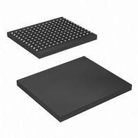
Page 31
... Document Number: 38-05540 Rev. *K Figure 12. 165-ball FBGA (13 × 15 × 1.4 mm) CY7C1360C, CY7C1362C 51-85180 *C Page [+] Feedback ...
Page 32
... TCK test clock TMS test mode select TDI test data-in TDO test data-out TQFP thin quad flat pack WE write enable Document Number: 38-05540 Rev. *K CY7C1360C, CY7C1362C Document Conventions Units of Measure Symbol Unit of Measure ns nano seconds V Volts µA micro Amperes mA milli Amperes ...
Page 33
... Document History Page Document Title: CY7C1360C/CY7C1362C 9-Mbit (256 K × 36/512 K × 18) Pipelined SRAM Document Number: 38-05540 Submission REV. ECN NO. Date ** 241690 See ECN *A 278130 See ECN *B 248929 See ECN *C 323636 See ECN *D 332879 See ECN *E 357258 See ECN *F 377095 See ECN ...
Page 34
... Document History Page (continued) Document Title: CY7C1360C/CY7C1362C 9-Mbit (256 K × 36/512 K × 18) Pipelined SRAM Document Number: 38-05540 Submission REV. ECN NO. Date *I 2756340 08/26/2009 *J 3046851 10/04/2010 *K 3052882 10/11/2010 Sales, Solutions, and Legal Information Worldwide Sales and Design Support Cypress maintains a worldwide network of offices, solution centers, manufacturer’s representatives, and distributors. To find the office ...