ES1D MULTICOMP, ES1D Datasheet
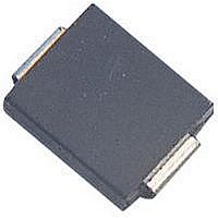
FAST DIODE, 1A, 200V, DO-214AC

ES1D

Manufacturer Part Number
ES1D
Description
FAST DIODE, 1A, 200V, DO-214AC
Manufacturer
MULTICOMP
Datasheet

Specifications of ES1D

Repetitive Reverse Voltage Vrrm Max
200V
Forward Current If(av)
1A
Forward Voltage Vf Max
950mV
Reverse Recovery Time Trr Max
35ns
Forward Surge Current Ifsm Max
30A
Diode Type
Fast Recovery
Lead Free Status / RoHS Status
Lead free / RoHS Compliant

Available stocks

Company
Part Number
Manufacturer
Quantity
Price
Part Number:
ES1D
Manufacturer:
FSC
Quantity:
127 500
Part Number:
ES1D
Manufacturer:
PANJIT/ 强茂
Quantity:
20 000
Part Number:
ES1D
Quantity:
6 200
Part Number:
ES1D
0
Company:
Part Number:
ES1D
Quantity:
39 858
Company:
Part Number:
ES1D
Quantity:
4 586
Part Number:
ES1D+
Manufacturer:
PANASONIC
Quantity:
712
Part Number:
ES1D-13-F
Manufacturer:
DIODES
Quantity:
50 000
Part Number:
ES1D-13-F
Manufacturer:
YEONHO
Quantity:
3 022
Part Number:
ES1D-13-F
Manufacturer:
DIODES
Quantity:
180
Part Number:
ES1D-13-F
Manufacturer:
DIODES/美台
Quantity:
20 000
Company:
Part Number:
ES1D-13-F
Quantity:
5 000
Company:
Part Number:
ES1D-13-F
Quantity:
935
Company:
Part Number:
ES1D-13-F
Quantity:
935
Part Number:
ES1D-AU
Manufacturer:
PANJIT/强茂
Quantity:
20 000
Part Number:
ES1D-AU_R1
Manufacturer:
PANJIT
Quantity:
19 253
Part Number:
ES1D-E3/11T
Manufacturer:
DELTA
Quantity:
3 823
Part Number:
ES1D-E3/11T
Manufacturer:
VISHAY/威世
Quantity:
20 000
Low Noise, Low Power, I
The ISL22313 integrates a single digitally controlled
potentiometer (DCP), control logic and non-volatile memory
on a monolithic CMOS integrated circuit.
The digitally controlled potentiometer is implemented with a
combination of resistor elements and CMOS switches. The
position of the wipers are controlled by the user through the
I
volatile Wiper Register (WR) and a non-volatile Initial Value
Register (IVR) that can be directly written to and read by the
user. The contents of the WR control the position of the
wiper. At power up the device recalls the contents of the
DCP’s IVR to the WR.
The ISL22313 also has 14 general purpose non-volatile
registers that can be used as storage of lookup table for
multiple wiper position or any other valuable information.
The ISL22313 features a dual supply, that is beneficial for
applications requiring a bipolar range for DCP terminals
between V- and VCC.
The DCP can be used as a three-terminal potentiometer or
as a two-terminal variable resistor in a wide variety of
applications including control, parameter adjustments, and
signal processing.
Pinout
Ordering Information
NOTES:
ISL22313TFU10Z
ISL22313UFU10Z
ISL22313WFU10Z
2
1. Intersil Pb-free plus anneal products employ special Pb-free material sets; molding compounds/die attach materials and 100% matte tin plate
2. Add “-TK” suffix for 1,000 Tape and Reel option
C bus interface. The potentiometer has an associated
termination finish, which are RoHS compliant and compatible with both SnPb and Pb-free soldering operations. Intersil Pb-free products are
MSL classified at Pb-free peak reflow temperatures that meet or exceed the Pb-free requirements of IPC/JEDEC J STD-020.
(Notes 1, 2)
NUMBER
PART
SDA
SCL
A1
A0
V-
1
2
3
4
5
(10 LD MSOP)
TOP VIEW
O
ISL22313
313TZ
313UZ
313WZ
®
MARKING
1
PART
2
C
10
Data Sheet
9
8
7
6
Single Digitally Controlled Potentiometer (XDCP™)
®
Bus, 256 Taps
VCC
RH
RW
RL
GND
RESISTANCE
1-888-INTERSIL or 1-888-468-3774
OPTION
(kΩ)
100
50
10
CAUTION: These devices are sensitive to electrostatic discharge; follow proper IC Handling Procedures.
-40 to +125
-40 to +125
-40 to +125
Features
• 256 resistor taps
• I
• Non-volatile EEPROM storage of wiper position
• 14 General Purpose non-volatile registers
• High reliability
• Wiper resistance: 70Ω typical @ 1mA
• Standby current <2.5µA max
• Shutdown current <2.5µA max
• Dual power supply
• DCP terminal voltage from V- to VCC
• 10kΩ, 50kΩ or 100kΩ total resistance
• Extended industrial temperature range: -40 to +125
• 10 Lead MSOP
• Pb-free plus anneal product (RoHS compliant)
RANGE
TEMP.
(°C)
|
- Two address pins, up to four devices per bus
- Endurance: 1,000,000 data changes per bit per register
- Register data retention: 50 years @ T≤+55
- VCC = 2.25V to 5.5V
- V- = -2.25V to -5.5V
2
Intersil (and design) and XDCP are registered trademarks of Intersil Americas Inc.
C serial interface
All other trademarks mentioned are the property of their respective owners.
July 17, 2007
10 Ld MSOP
10 Ld MSOP
10 Ld MSOP
Copyright Intersil Americas Inc. 2007. All Rights Reserved
PACKAGE
(Pb-Free)
ISL22313
M10.118
M10.118
M10.118
PKG. DWG. #
FN6421.0
°
C
°
C

Related parts for ES1D

ES1D Summary of contents

Page 1

Single Digitally Controlled Potentiometer (XDCP™) Data Sheet 2 ® Low Noise, Low Power The ISL22313 integrates a single digitally controlled potentiometer (DCP), control logic and non-volatile memory on a monolithic CMOS integrated circuit. The digitally controlled potentiometer ...

Page 2

Block Diagram SCL SDA A1 INTERFACE A0 Pin Descriptions MSOP PIN SYMBOL 1 SCL 2 SDA GND VCC 2 ISL22313 V CC POWER UP INTERFACE, 2 ...

Page 3

Absolute Maximum Ratings Storage Temperature . . . . . . . . . . . . . . . . . . . . . . . .-65°C to +150°C Voltage at any Digital Interface Pin with Respect to ...

Page 4

Analog Specifications Over recommended operating conditions unless otherwise stated. Limits are established by characterization. (Continued) SYMBOL PARAMETER f -3dB cut off frequency cutoff (Note 16) RESISTOR MODE (Measurements between RW and RL with RH not connected, or between RW and ...

Page 5

Operating Specifications Over the recommended operating conditions unless otherwise specified. Limits are established by characterization. (Continued) SYMBOL PARAMETER I V Current (standby Current (standby) V- Current (shutdown Current (standby) V-SB ...

Page 6

Operating Specifications Over the recommended operating conditions unless otherwise specified. Limits are established by characterization. (Continued) SYMBOL PARAMETER SERIAL INTERFACE SPECS V A1, A0, SDA, and SCL input buffer IL LOW voltage V A1, A0, SDA, and SCL input buffer ...

Page 7

Operating Specifications Over the recommended operating conditions unless otherwise specified. Limits are established by characterization. (Continued) SYMBOL PARAMETER t A1 and A0 setup time SU and A0 hold time HD:A NOTES: 4. Typical values are for T = ...

Page 8

A0 and A1 Pin Timing START SCL SDA A0, A1 Typical Performance Curves 100 150 TAP POSITION (DECIMAL) FIGURE 1. WIPER RESISTANCE vs TAP POSITION [ I(RW ...

Page 9

Typical Performance Curves 2.0 1.6 1.2 0.8 50k V = 2.25V CC 0 TEMPERATURE (ºC) FIGURE 5. ZS ERROR vs TEMPERATURE 0 5.5V CC 0.25 0 -0. 2.25V CC -0. ...

Page 10

Typical Performance Curves 500 10k 400 300 200 100 116 TAP POSITION (DECIMAL) FIGURE 11. TC FOR RHEOSTAT MODE IN ppm SCL WIPER FIGURE 13. MIDSCALE GLITCH, CODE 7Fh TO 80h Pin Description Potentiometers Pins RH and ...

Page 11

Device Address (A1, A0) The address inputs are used to set the least significant 2 bits 2 of the 7-bit I C interface slave address. A match in the slave address serial data stream must match with the Address input ...

Page 12

FIGURE 15. DCP CONNECTION IN SHUTDOWN MODE The WIP bit (ACR[5 read-only bit. It indicates that non- volatile write operation is in progress impossible to write to the WR or ACR while WIP ...

Page 13

SCL FROM MASTER SDA OUTPUT FROM TRANSMITTER SDA OUTPUT FROM RECEIVER START FIGURE 17. ACKNOWLEDGE RESPONSE FROM RECEIVER SIGNALS FROM THE MASTER SIGNAL AT SDA SIGNALS FROM THE SLAVE S SIGNALS T FROM THE A IDENTIFICATION MASTER R BYTE WITH ...

Page 14

Data Byte. After reaching the memory location 0Fh, the pointer “rolls over” to 00h, and the device continues to output data for each ACK received.The master terminates the read operation issuing a NACK ...

Page 15

Mini Small Outline Plastic Packages (MSOP -B- INDEX 1 2 0.20 (0.008) AREA TOP VIEW 0.25 (0.010) GAUGE PLANE SEATING PLANE - 0.10 (0.004) b -H- - 0.20 (0.008) SIDE VIEW 0.20 ...

Related keywords