FDP036N10A Fairchild Semiconductor, FDP036N10A Datasheet

MOSFET N-CH 100V TO-220AB-3

FDP036N10A

Manufacturer Part Number
FDP036N10A
Description
MOSFET N-CH 100V TO-220AB-3
Manufacturer
Fairchild Semiconductor
Series
PowerTrench®r
Datasheet

Specifications of FDP036N10A

Fet Type
MOSFET N-Channel, Metal Oxide
Fet Feature
Standard
Rds On (max) @ Id, Vgs
3.6 mOhm @ 75A, 10V
Drain To Source Voltage (vdss)
100V
Current - Continuous Drain (id) @ 25° C
120A
Vgs(th) (max) @ Id
4V @ 250µA
Gate Charge (qg) @ Vgs
116nC @ 10V
Input Capacitance (ciss) @ Vds
7295pF @ 25V
Power - Max
227W
Mounting Type
Through Hole
Package / Case
TO-220-3 Formed Leads
Configuration
Single
Transistor Polarity
N-Channel
Resistance Drain-source Rds (on)
3.6 mOhms
Forward Transconductance Gfs (max / Min)
167 S
Drain-source Breakdown Voltage
100 V
Gate-source Breakdown Voltage
20 V
Continuous Drain Current
176 A
Power Dissipation
227 W
Maximum Operating Temperature
+ 150 C
Mounting Style
Through Hole
Gate Charge Qg
89 nC
Minimum Operating Temperature
- 55 C
Continuous Drain Current Id
214A
Drain Source Voltage Vds
100V
On Resistance Rds(on)
0.0032ohm
Rds(on) Test Voltage Vgs
10V
Lead Free Status / RoHS Status
Lead free / RoHS Compliant

Available stocks

Company
Part Number
Manufacturer
Quantity
Price
Part Number:
FDP036N10A
Manufacturer:
FAIRCHILD
Quantity:
10 000
Part Number:
FDP036N10A
Manufacturer:
FAIRCHILD/仙童
Quantity:
20 000
Company:
Part Number:
FDP036N10A
Quantity:
7 000
©2010 Fairchild Semiconductor Corporation
FDP036N10A Rev. A1
MOSFET Maximum Ratings
*Calculated continuous current based on maximum allowable junction temperature. Package limitation current is 120A.
Thermal Characteristics
V
V
I
I
E
dv/dt
P
T
T
R
R
D
DM
FDP036N10A
N-Channel PowerTrench
100V, 176A, 3.6mW
Features
• R
• Fast Switching Speed
• Low Gate Charge
• High Performance Trench Technology for Extremely Low
• High Power and Current Handling Capability
• RoHS Compliant
J
L
DSS
GSS
AS
D
qJC
qJA
, T
Symbol
Symbol
R
STG
DS(on)
DS(on)
= 3.2mW ( Typ.)@ V
Drain to Source Voltage
Gate to Source Voltage
Drain Current
Drain Current
Single Pulsed Avalanche Energy
Peak Diode Recovery dv/dt
Power Dissipation
Operating and Storage Temperature Range
Maximum Lead Temperature for Soldering Purpose,
1/8” from Case for 5 Seconds
Thermal Resistance, Junction to Case
Thermal Resistance, Junction to Ambient
(FLANGE)
DRAIN
GS
= 10V, I
FDP Series
TO-220AB
D
= 75A
T
C
= 25
Parameter
Parameter
- Continuous (T
- Continuous (T
- Continuous (T
- Pulsed
(T
- Derate above 25
®
C
o
C unless otherwise noted
= 25
MOSFET
GATE
DRAIN
SOURCE
o
C)
C
C
C
= 25
= 100
= 25
1
o
C
Description
This N-Channel MOSFET is produced using Fairchild Semicon-
ductor’s advanced PowerTrench process that has been espe-
cially tailored to minimize the on-state resistance and yet
maintain superior switching performance.
Application
• DC to DC Convertors / Synchronous Rectification
o
o
C, Silicon Limited)
C, Package Limited)
o
C, Silicon Limited)
(Note 1)
(Note 2)
(Note 3)
G
S
D
-55 to +175
Ratings
Ratings
176*
125*
0.66
62.5
100
±20
120
704
558
227
300
6.0
1.5
www.fairchildsemi.com
July 2010
Units
W/
Units
V/ns
o
mJ
o
o
C/W
W
V
V
A
A
C
C
o
C

Related parts for FDP036N10A

FDP036N10A Summary of contents

Page 1

... Symbol R Thermal Resistance, Junction to Case qJC R Thermal Resistance, Junction to Ambient qJA ©2010 Fairchild Semiconductor Corporation FDP036N10A Rev. A1 ® MOSFET Description = 75A This N-Channel MOSFET is produced using Fairchild Semicon- D ductor’s advanced PowerTrench process that has been espe- cially tailored to minimize the on-state resistance and yet maintain superior switching performance ...

Page 2

... Starting T = 25° 0.31mH 60A J AS £ 75A, di/dt £ 200A/ms, V £ Starting DSS 4. Pulse Test: Pulse width £ 300ms, Duty Cycle £ Essentially Independent of Operating Temperature Typical Characteristics FDP036N10A Rev. A1 Package Reel Size TO-220 - unless otherwise noted C Test Conditions I = 250mA 0V, T ...

Page 3

... GS 0.0025 0 60 120 180 I , Drain Current [A] D Figure 5. Capacitance Characteristics 10000 C iss = oss = rss = C gd 5000 100 0 Drain-Source Voltage [V] DS FDP036N10A Rev. A1 Figure 2. Transfer Characteristics 300 100 *Notes: 1. 250 m s Pulse Test Figure 4. Body Diode Forward Voltage 500 100 o *Note ...

Page 4

... Figure 11. Unclamped Inductive Switching Capability 200 ( 1.3*RATED 100 (L/R) STARTING T = 150 0.01 0 TIME IN AVALANCHE (ms) AV FDP036N10A Rev. A1 Figure 8. On-Resistance Variation 2.1 1.8 1.5 1.2 0.9 *Notes 10mA D 0.6 100 150 200 Figure 10. Maximum Drain Current 200 m 100 s 150 1ms 10ms 100ms 100 DC 50 ...

Page 5

... Typical Performance Characteristics 3 1 0.5 0.2 0.1 0.1 0.05 0.02 0.01 0.01 Single pulse 0.001 -5 10 FDP036N10A Rev. A1 Figure 12. Transient Thermal Response Curve P *Notes Duty Factor Rectangular Pulse Duration [sec (t) = 0.66 C/W Max ( www.fairchildsemi.com ...

Page 6

... FDP036N10A Rev. A1 Gate Charge Test Circuit & Waveform Resistive Switching Test Circuit & Waveforms Unclamped Inductive Switching Test Circuit & Waveforms 6 www.fairchildsemi.com ...

Page 7

... Driver ) ( Driver ) DUT ) ( DUT ) DUT ) ( DUT ) FDP036N10A Rev. A1 Peak Diode Recovery dv/dt Test Circuit & Waveforms + + DUT DUT Driver Driver Same Type Same Type as DUT as DUT GS GS • dv/dt controlled by R • dv/dt controlled by R • I • I controlled by pulse period controlled by pulse period ...

Page 8

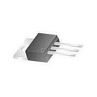
... Mechanical Dimensions FDP036N10A Rev. A1 TO-220AB 8 www.fairchildsemi.com ...

Page 9

... Definition of Terms Datasheet Identification Product Status Advance Information Formative / In Design Preliminary First Production No Identification Needed Full Production Obsolete Not In Production FDP036N10A Rev. A1 F-PFS™ Power-SPM™ ® FRFET PowerTrench SM Global Power Resource PowerXS™ Green FPS™ Programmable Active Droop™ ...

Related keywords