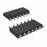
LF398M/NOPB National Semiconductor, LF398M/NOPB Datasheet - Page 7

LF398M/NOPB
Manufacturer Part Number
LF398M/NOPB
Description
IC AMP MONO SAMPLE & HOLD 14SOIC
Manufacturer
National Semiconductor
Datasheet
1.LF398NNOPB.pdf
(13 pages)
Specifications of LF398M/NOPB
Amplifier Type
Sample and Hold
Number Of Circuits
1
Current - Input Bias
10nA
Voltage - Input Offset
2000µV
Current - Supply
4.5mA
Voltage - Supply, Single/dual (±)
±5 V ~ 18 V
Operating Temperature
0°C ~ 70°C
Mounting Type
Surface Mount
Package / Case
14-SOIC (3.9mm Width), 14-SOL
Acquisition Time
4 us
Maximum Operating Temperature
+ 70 C
Minimum Operating Temperature
0 C
Supply Voltage (max)
18 V
Supply Voltage (min)
5 V
Lead Free Status / RoHS Status
Lead free / RoHS Compliant
Output Type
-
Current - Output / Channel
-
-3db Bandwidth
-
Slew Rate
-
Gain Bandwidth Product
-
Lead Free Status / Rohs Status
Details
Other names
*LF398M
*LF398M/NOPB
LF398M
*LF398M/NOPB
LF398M
Available stocks
Company
Part Number
Manufacturer
Quantity
Price
Part Number:
LF398M/NOPB
Manufacturer:
NS/国半
Quantity:
20 000
Application Hints
(Continued)
Guarding Technique
logic input for signal delay, calculate the slope of the wave-
form at the threshold point to ensure that it is at least
1.0 V/µs.
Sampling Dynamic Signals
Sample error to moving input signals probably causes more
confusion among sample-and-hold users than any other pa-
rameter. The primary reason for this is that many users make
the assumption that the sample and hold amplifier is truly
locked on to the input signal while in the sample mode. In ac-
tuality, there are finite phase delays through the circuit creat-
ing an input-output differential for fast moving signals. In ad-
dition, although the output may have settled, the hold
capacitor has an additional lag due to the 300 series resis-
tor on the chip. This means that at the moment the “hold”
command arrives, the hold capacitor voltage may be some-
what different than the actual analog input. The effect of
these delays is opposite to the effect created by delays in the
logic which switches the circuit from sample to hold. For ex-
DS005692-5
ample, consider an analog input of 20 Vp-p at 10 kHz. Maxi-
Use 10-pin layout. Guard around C
is tied to output.
mum dV/dt is 0.6 V/µs. With no analog phase delay and 100
h
ns logic delay, one could expect up to (0.1 µs) (0.6V/µs)
= 60 mVerror if the “hold” signal arrived near maximum dV/dt
of the input. A positive-going input would give a +60 mV er-
ror. Now assume a 1 MHz (3 dB) bandwidth for the overall
analog loop. This generates a phase delay of 160 ns. If the
hold capacitor sees this exact delay, then error due to analog
delay will be (0.16 µs) (0.6 V/µs) = −96 mV. Total output error
is +60 mV (digital) −96 mV (analog) for a total of −36 mV. To
add to the confusion, analog delay is proportioned to hold
capacitor value while digital delay remains constant. A family
of curves (dynamic sampling error) is included to help esti-
mate errors.
A curve labeled Aperture Time has been included for sam-
pling conditions where the input is steady during the sam-
pling period, but may experience a sudden change nearly
coincident with the “hold” command. This curve is based on
a 1 mV error fed into the output.
A second curve, Hold Settling Time indicates the time re-
quired for the output to settle to 1 mV after the “hold” com-
mand.
Digital Feedthrough
Fast rise time logic signals can cause hold errors by feeding
externally into the analog input at the same time the amplifier
is put into the hold mode. To minimize this problem, board
layout should keep logic lines as far as possible from the
analog input and the C
pin. Grounded guarding traces may
h
also be used around the input line, especially if it is driven
from a high impedance source. Reducing high amplitude
logic signals to 2.5V will also help.
7
www.national.com


