LF398M/NOPB National Semiconductor, LF398M/NOPB Datasheet - Page 3
LF398M/NOPB
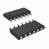
Manufacturer Part Number
LF398M/NOPB
Description
IC AMP MONO SAMPLE & HOLD 14SOIC
Manufacturer
National Semiconductor
Datasheet
1.LF398NNOPB.pdf
(13 pages)
Specifications of LF398M/NOPB
Amplifier Type
Sample and Hold
Number Of Circuits
1
Current - Input Bias
10nA
Voltage - Input Offset
2000µV
Current - Supply
4.5mA
Voltage - Supply, Single/dual (±)
±5 V ~ 18 V
Operating Temperature
0°C ~ 70°C
Mounting Type
Surface Mount
Package / Case
14-SOIC (3.9mm Width), 14-SOL
Acquisition Time
4 us
Maximum Operating Temperature
+ 70 C
Minimum Operating Temperature
0 C
Supply Voltage (max)
18 V
Supply Voltage (min)
5 V
Lead Free Status / RoHS Status
Lead free / RoHS Compliant
Output Type
-
Current - Output / Channel
-
-3db Bandwidth
-
Slew Rate
-
Gain Bandwidth Product
-
Lead Free Status / Rohs Status
Details
Other names
*LF398M
*LF398M/NOPB
LF398M
*LF398M/NOPB
LF398M
Available stocks
Company
Part Number
Manufacturer
Quantity
Price

Part Number:
LF398M/NOPB
Manufacturer:
NS/国半
Quantity:
20 000


Input Impedance
Gain Error
Feedthrough Attenuation Ratio
at 1 kHz
Output Impedance
“HOLD” Step, (Note 6)
Supply Current, (Note 5)
Logic and Logic Reference Input
Current
Leakage Current into Hold
Capacitor (Note 5)
Acquisition Time to 0.1%
Hold Capacitor Charging Current
Supply Voltage Rejection Ratio
Differential Logic Threshold
The following specifcations apply for −V
R
Electrical Characteristics
Note 1: “Absolute Maximum Ratings” indicate limits beyond which damage to the device may occur. Operating Ratings indicate conditions for which the device is
functional, but do not guarantee specific performance limits.
Note 2: The maximum power dissipation must be derated at elevated temperatures and is dictated by T
allowable power dissipation at any temperature is P
junction temperature, T
Note 3: Although the differential voltage may not exceed the limits given, the common-mode voltage on the logic pins may be equal to the supply voltages without
causing damage to the circuit. For proper logic operation, however, one of the logic pins must always be at least 2V below the positive supply and 3V above the nega-
tive supply.
Note 4: See AN-450 “Surface Mounting Methods and their effects on Product Reliability” for other methods of soldering surface mount devices.
Note 5: These parameters guaranteed over a supply voltage range of
Note 6: Hold step is sensitive to stray capacitive coupling between input logic signals and the hold capacitor. 1 pF, for instance, will create an additional 0.5 mV step
with a 5V logic swing and a 0.01µF hold capacitor. Magnitude of the hold step is inversely proportional to hold capacitor value.
Note 7: Leakage current is measured at a junction temperature of 25˚C. The effects of junction temperature rise due to power dissipation or elevated ambient can
be calculated by doubling the 25˚C value for each 11˚C increase in chip temperature. Leakage is guaranteed over full input signal range.
Note 8: A military RETS electrical test specification is available on request. The LF198 may also be procured to Standard Military Drawing # 5962-8760801GA or to
MIL-STD-38510 part ID JM38510/12501SGA.
Typical Performance Characteristics
Aperture Time
(Note 9)
Note 9: See Definition of Terms
L
= 10 k , LOGIC REFERENCE = 0V, LOGIC HIGH = 2.5V, LOGIC LOW = 0V unless otherwise specified.
Parameter
JMAX
, for the LF198/LF198A is 150˚C; for the LF298, 115˚C; and for the LF398/LF398A, 100˚C.
DS005692-17
T
T
Full Temperature Range
T
T
Full Temperature Range
T
T
T
T
Hold Mode
C
V
V
T
j
j
j
j
j
j
j
j
V
j
IN
OUT
h
= 25˚C
= 25˚C, R
= 25˚C, C
= 25˚C, “HOLD” mode
= 25˚C, C
= 25˚C
= 25˚C, (Note 7)
= 25˚C
OUT
25˚C
−V
= 0.01 µF
S
D
+ 3.5V
OUT
= 0
= (T
= 10V, C
Dielectric Absorption
Error in Hold Capacitor
JMAX
= 2V
Conditions
L
h
h
− T
= 10k
= 0.01 µF
= 0.01µF, V
V
A
IN
h
)/
= 1000 pF
JA
±
, or the number given in the Absolute Maximum Ratings, whichever is lower. The maximum
+V
5 to
S
±
− 3.5V, +V
OUT
18V, and an input range of −V
3
= 0
S
= +15V, −V
DS005692-18
Min
0.8
86
90
JMAX
LF198A
0.002
10
Typ
110
0.5
0.5
4.5
1.4
96
30
20
2
4
5
,
10
S
S
JA
+ 3.5V
= −15V, T
Dynamic Sampling Error
, and the ambient temperature, T
0.005
Max
0.01
100
5.5
2.4
10
25
1
4
1
6
V
IN
A
+V
Min
= T
0.8
86
90
S
− 3.5V.
j
= 25˚C, C
LF398A
0.004
10
Typ
110
0.5
1.0
4.5
1.4
90
30
20
2
4
5
10
A
0.005
h
. The maximum
Max
0.01
www.national.com
100
6.5
2.4
10
25
= 0.01 µF,
1
6
1
6
DS005692-19
Units
mV
mA
mA
dB
µA
pA
dB
µs
µs
%
%
V
Related parts for LF398M/NOPB
Image
Part Number
Description
Manufacturer
Datasheet
Request
R

Part Number:
Description:
AMP, MONO, SAMPLE & HOLD, 14SOIC
Manufacturer:
National Semiconductor
Datasheet:

Part Number:
Description:
National Semiconductor [8-Bit D/A Converter]
Manufacturer:
National Semiconductor
Datasheet:
Part Number:
Description:
National Semiconductor [Media Coprocessor]
Manufacturer:
National Semiconductor
Datasheet:
Part Number:
Description:
Digitally Controlled Tone and Volume Circuit with Stereo Audio Power Amplifier, Microphone Preamp Stage and National 3D Sound
Manufacturer:
National Semiconductor
Datasheet:
Part Number:
Description:
Digitally Controlled Tone and Volume Circuit with Stereo Audio Power Amplifier, Microphone Preamp Stage and National 3D Sound
Manufacturer:
National Semiconductor
Datasheet:
Part Number:
Description:
AC97 Rev 2 Codec with Sample Rate Conversion and National 3D Sound
Manufacturer:
National Semiconductor
Part Number:
Description:
Manufacturer:
National Semiconductor
Datasheet:
Part Number:
Description:
Manufacturer:
National Semiconductor
Datasheet:
Part Number:
Description:
General Purpose, Low Voltage, Low Power, Rail-to-Rail Output Operational Amplifiers
Manufacturer:
National Semiconductor
Datasheet:
Part Number:
Description:
8-bit 20 MSPS flash A/D converter.
Manufacturer:
National Semiconductor
Datasheet:
Part Number:
Description:
Low Noise Quad Operational Amplifier
Manufacturer:
National Semiconductor
Datasheet:
Part Number:
Description:
Quad Differential Line Receivers
Manufacturer:
National Semiconductor
Datasheet:
Part Number:
Description:
Quad High Speed Trapezoidal? Bus Transceiver
Manufacturer:
National Semiconductor
Datasheet:
Part Number:
Description:
Dual Line Receiver
Manufacturer:
National Semiconductor
Datasheet: