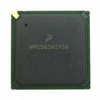
MPC562MZP56 Freescale Semiconductor, MPC562MZP56 Datasheet - Page 902

MPC562MZP56
Manufacturer Part Number
MPC562MZP56
Description
IC MPU 32BIT 56MHZ PPC 388-PBGA
Manufacturer
Freescale Semiconductor
Series
MPC5xxr
Datasheet
1.MPC561MZP56.pdf
(1420 pages)
Specifications of MPC562MZP56
Core Processor
PowerPC
Core Size
32-Bit
Speed
56MHz
Connectivity
CAN, EBI/EMI, SCI, SPI, UART/USART
Peripherals
POR, PWM, WDT
Number Of I /o
64
Program Memory Type
ROMless
Ram Size
32K x 8
Voltage - Supply (vcc/vdd)
2.5 V ~ 2.7 V
Data Converters
A/D 32x10b
Oscillator Type
External
Operating Temperature
-40°C ~ 125°C
Package / Case
388-BGA
Processor Series
MPC5xx
Core
PowerPC
Data Bus Width
32 bit
Data Ram Size
8 KB
Interface Type
SCI, SPI, UART
Maximum Clock Frequency
40 MHz
Number Of Programmable I/os
56
Number Of Timers
22
Operating Supply Voltage
2.6 V to 5 V
Maximum Operating Temperature
+ 85 C
Mounting Style
SMD/SMT
Minimum Operating Temperature
- 40 C
On-chip Adc
2 (10 bit, 32 Channel)
For Use With
MPC564EVB - KIT EVAL FOR MPC561/562/563/564
Lead Free Status / RoHS Status
Request inventory verification / Request inventory verification
Eeprom Size
-
Program Memory Size
-
Lead Free Status / Rohs Status
No
Available stocks
Company
Part Number
Manufacturer
Quantity
Price
Company:
Part Number:
MPC562MZP56
Manufacturer:
FREESCAL
Quantity:
204
Company:
Part Number:
MPC562MZP56
Manufacturer:
Freescale Semiconductor
Quantity:
10 000
Part Number:
MPC562MZP56
Manufacturer:
FREESCALE
Quantity:
20 000
Company:
Part Number:
MPC562MZP56R2
Manufacturer:
RFT
Quantity:
1 441
Company:
Part Number:
MPC562MZP56R2
Manufacturer:
Freescale Semiconductor
Quantity:
10 000
- Current page: 902 of 1420
- Download datasheet (11Mb)
CALRAM Operation
22.4.5
Stop Operation
The low power stop mode for this module is entered by setting the disable bit (DIS) in the CRAMMCR
register. Reads from and writes to the array during this mode will generate an error.
When the disable bit (DIS) is cleared, the module returns to normal function.
22.4.6
Overlay Mode Operation
For a microcontroller used as a controller for an engine (or other electromechanical device), various
parameters stored in the Flash memory may need to be changed in order to properly tune (calibrate) the
engine. Because Flash memory may not be readily programmed during normal operation of an embedded
controller, portions of the CALRAM array can be overlayed onto the U-bus Flash memory. By allowing
the CALRAM module to overlay portions of Flash memory, parameters normally stored in the Flash may
be tweaked and changed with a development tool both during normal operation and prior to programming
a final, more precise version of the Flash memory.
The overlay is for read-only data and does not affect instruction fetches from the Flash. The data for any
L-bus address which falls in the overlay region of the U-bus Flash will be driven by the CALRAM on the
L-bus. The CALRAM also indicates to the L2U to block the data from the Flash to be driven onto the
L-bus. As far as the RCPU core is concerned, the timing of data coming from the CALRAM appears to be
the same as that from the Flash.
22.4.6.1
Overlay Mode Configuration
Each CALRAM module contains eight overlay regions, each of which is 512 bytes long as shown in
Figure
22-4. All overlay regions of a module are contiguous and each starts at the least significant address
of the region and can increment all the way up to 512 bytes as shown in
Figure
22-5. As described in
section
Section 22.5.2, “CALRAM Region Base Address Registers
(CRAM_RBAx)”, CRAM_RBAx
registers allow the programming of the base addresses RBA[11:29] of the U-bus Flash regions and the
RGN_SIZE[0:4] to be overlaid. Note that each region can also be individually disabled by writing 0000 to
RGN_SIZE[0:3]. If the programmed base address is not naturally aligned with respect to the RGN_SIZE
field, the least significant bits of the base address fields can be considered 0’s in order to make the starting
address naturally aligned. In an RBA register, RGN_SIZE[0:3] ={0101} select the size to be 128 bytes,
and even if CRAM_RBAx [25:29] are not all 0’s, they will be considered as 0’s so that the address
becomes 128-byte naturally aligned.
MPC561/MPC563 Reference Manual, Rev. 1.2
22-6
Freescale Semiconductor
Related parts for MPC562MZP56
Image
Part Number
Description
Manufacturer
Datasheet
Request
R
Part Number:
Description:
Mpc562 32 Bit Powerpc Microcontroller
Manufacturer:
Freescale Semiconductor, Inc
Datasheet:

Part Number:
Description:
MPC5 1K0 5%
Manufacturer:
TE Connectivity
Datasheet:

Part Number:
Description:
MPC5 500R 5%
Manufacturer:
TE Connectivity
Datasheet:

Part Number:
Description:
MPC5 5K0 5%
Manufacturer:
Tyco Electronics
Datasheet:

Part Number:
Description:
MPC5 5R0 5%
Manufacturer:
Tyco Electronics
Datasheet:

Part Number:
Description:
MPC5 50K 5%
Manufacturer:
Tyco Electronics
Datasheet:
Part Number:
Description:
Manufacturer:
Freescale Semiconductor, Inc
Datasheet:
Part Number:
Description:
Manufacturer:
Freescale Semiconductor, Inc
Datasheet:
Part Number:
Description:
Manufacturer:
Freescale Semiconductor, Inc
Datasheet:
Part Number:
Description:
Manufacturer:
Freescale Semiconductor, Inc
Datasheet:
Part Number:
Description:
Manufacturer:
Freescale Semiconductor, Inc
Datasheet:


