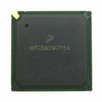
MPC562MZP56 Freescale Semiconductor, MPC562MZP56 Datasheet - Page 877

MPC562MZP56
Manufacturer Part Number
MPC562MZP56
Description
IC MPU 32BIT 56MHZ PPC 388-PBGA
Manufacturer
Freescale Semiconductor
Series
MPC5xxr
Datasheet
1.MPC561MZP56.pdf
(1420 pages)
Specifications of MPC562MZP56
Core Processor
PowerPC
Core Size
32-Bit
Speed
56MHz
Connectivity
CAN, EBI/EMI, SCI, SPI, UART/USART
Peripherals
POR, PWM, WDT
Number Of I /o
64
Program Memory Type
ROMless
Ram Size
32K x 8
Voltage - Supply (vcc/vdd)
2.5 V ~ 2.7 V
Data Converters
A/D 32x10b
Oscillator Type
External
Operating Temperature
-40°C ~ 125°C
Package / Case
388-BGA
Processor Series
MPC5xx
Core
PowerPC
Data Bus Width
32 bit
Data Ram Size
8 KB
Interface Type
SCI, SPI, UART
Maximum Clock Frequency
40 MHz
Number Of Programmable I/os
56
Number Of Timers
22
Operating Supply Voltage
2.6 V to 5 V
Maximum Operating Temperature
+ 85 C
Mounting Style
SMD/SMT
Minimum Operating Temperature
- 40 C
On-chip Adc
2 (10 bit, 32 Channel)
For Use With
MPC564EVB - KIT EVAL FOR MPC561/562/563/564
Lead Free Status / RoHS Status
Request inventory verification / Request inventory verification
Eeprom Size
-
Program Memory Size
-
Lead Free Status / Rohs Status
No
Available stocks
Company
Part Number
Manufacturer
Quantity
Price
Company:
Part Number:
MPC562MZP56
Manufacturer:
FREESCAL
Quantity:
204
Company:
Part Number:
MPC562MZP56
Manufacturer:
Freescale Semiconductor
Quantity:
10 000
Part Number:
MPC562MZP56
Manufacturer:
FREESCALE
Quantity:
20 000
Company:
Part Number:
MPC562MZP56R2
Manufacturer:
RFT
Quantity:
1 441
Company:
Part Number:
MPC562MZP56R2
Manufacturer:
Freescale Semiconductor
Quantity:
10 000
- Current page: 877 of 1420
- Download datasheet (11Mb)
21.2.2
The UC3F array is divided into eight blocks, 64 Kbytes in size, which may be independently erased. Two
blocks are host to a 16-Kbyte small block.
Seventeen bits of address are used to decode locations in the UC3F array. The read control logic in the
UC3F EEPROM module decodes the upper 14 bits of that address to determine if the desired data is
currently stored in one of the two read page buffers. If the data is already present in one of the two read
page buffers, a read operation is not completed to the UC3F array core, and 64 bits of data are transferred
from the appropriate read page buffer to the BIU. This type of array read access is an on-page read.
In the event that the read control logic determines that the desired data is not contained within one of the
read page buffers, a read access to the UC3F array core is completed and 32 bytes of data are transferred
from the array core. Only the addressed 64 bits of data will be transferred to the BIU. This type of array
read access is an off-page read. The BIU contains logic to implement the read page buffer update and
replacement scheme to transfer the 32 bytes of data into the appropriate read page buffer. If the read page
update and replacement scheme contains a random access mode that does not update the read page buffers,
the 32 bytes of data retrieved from the UC3F array core will not be transferred into either read page buffer.
The BIU is expected to contain page update logic for controlling the updating of the read page buffers.
Write accesses to the UC3F array have no effect except during program and erase operation.
21.2.3
The UC3F EEPROM module contains a special shadow row that is used to hold reset configuration data
and user data. See
The shadow row is accessed by setting UC3FMCR[SIE] = 1 and performing normal array accesses. Upon
transitioning SIE (a 1-to-0 or 0-to-1 transition), the read page match decode circuit is reset so that the next
array access is an off-page access.
The shadow row contains 512 bytes which are addressed for read accesses using the low order row and
read page addresses.
The shadow row is implemented in the lowest numbered block of the array. In the case of a UC3F array
configuration which also has a small block in the lowest numbered block of the array, the shadow row is
contained in the small block. If SBEN[0] = 1 in this array configuration, the shadow row is treated as part
of small block 0. SBPROTECT[0] and SBBLOCK[0] are used to control program and erase operation of
the shadow row. If SBEN[0] = 0 in this array configuration, the shadow row is treated as part of the host
block. The corresponding PROTECT and BLOCK bits are used to control program and erase operation of
the shadow row.
Freescale Semiconductor
UC3F EEPROM Array Addressing
UC3F EEPROM Shadow Row
A module cannot read its own shadow row. On the MPC563 the program
accessing the Flash shadow row must be executing from external memory
or from internal SRAM.
Figure
21-6.
MPC561/MPC563 Reference Manual, Rev. 1.2
NOTE
CDR3 Flash (UC3F) EEPROM
21-15
Related parts for MPC562MZP56
Image
Part Number
Description
Manufacturer
Datasheet
Request
R
Part Number:
Description:
Mpc562 32 Bit Powerpc Microcontroller
Manufacturer:
Freescale Semiconductor, Inc
Datasheet:

Part Number:
Description:
MPC5 1K0 5%
Manufacturer:
TE Connectivity
Datasheet:

Part Number:
Description:
MPC5 500R 5%
Manufacturer:
TE Connectivity
Datasheet:

Part Number:
Description:
MPC5 5K0 5%
Manufacturer:
Tyco Electronics
Datasheet:

Part Number:
Description:
MPC5 5R0 5%
Manufacturer:
Tyco Electronics
Datasheet:

Part Number:
Description:
MPC5 50K 5%
Manufacturer:
Tyco Electronics
Datasheet:
Part Number:
Description:
Manufacturer:
Freescale Semiconductor, Inc
Datasheet:
Part Number:
Description:
Manufacturer:
Freescale Semiconductor, Inc
Datasheet:
Part Number:
Description:
Manufacturer:
Freescale Semiconductor, Inc
Datasheet:
Part Number:
Description:
Manufacturer:
Freescale Semiconductor, Inc
Datasheet:
Part Number:
Description:
Manufacturer:
Freescale Semiconductor, Inc
Datasheet:


