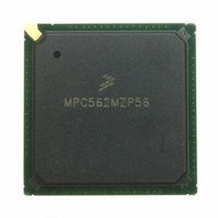
MPC562MZP56 Freescale Semiconductor, MPC562MZP56 Datasheet - Page 861

MPC562MZP56
Manufacturer Part Number
MPC562MZP56
Description
IC MPU 32BIT 56MHZ PPC 388-PBGA
Manufacturer
Freescale Semiconductor
Series
MPC5xxr
Datasheet
1.MPC561MZP56.pdf
(1420 pages)
Specifications of MPC562MZP56
Core Processor
PowerPC
Core Size
32-Bit
Speed
56MHz
Connectivity
CAN, EBI/EMI, SCI, SPI, UART/USART
Peripherals
POR, PWM, WDT
Number Of I /o
64
Program Memory Type
ROMless
Ram Size
32K x 8
Voltage - Supply (vcc/vdd)
2.5 V ~ 2.7 V
Data Converters
A/D 32x10b
Oscillator Type
External
Operating Temperature
-40°C ~ 125°C
Package / Case
388-BGA
Processor Series
MPC5xx
Core
PowerPC
Data Bus Width
32 bit
Data Ram Size
8 KB
Interface Type
SCI, SPI, UART
Maximum Clock Frequency
40 MHz
Number Of Programmable I/os
56
Number Of Timers
22
Operating Supply Voltage
2.6 V to 5 V
Maximum Operating Temperature
+ 85 C
Mounting Style
SMD/SMT
Minimum Operating Temperature
- 40 C
On-chip Adc
2 (10 bit, 32 Channel)
For Use With
MPC564EVB - KIT EVAL FOR MPC561/562/563/564
Lead Free Status / RoHS Status
Request inventory verification / Request inventory verification
Eeprom Size
-
Program Memory Size
-
Lead Free Status / Rohs Status
No
Available stocks
Company
Part Number
Manufacturer
Quantity
Price
Company:
Part Number:
MPC562MZP56
Manufacturer:
FREESCAL
Quantity:
204
Company:
Part Number:
MPC562MZP56
Manufacturer:
Freescale Semiconductor
Quantity:
10 000
Part Number:
MPC562MZP56
Manufacturer:
FREESCALE
Quantity:
20 000
Company:
Part Number:
MPC562MZP56R2
Manufacturer:
RFT
Quantity:
1 441
Company:
Part Number:
MPC562MZP56R2
Manufacturer:
Freescale Semiconductor
Quantity:
10 000
- Current page: 861 of 1420
- Download datasheet (11Mb)
20.4.3
When a synchronous reset occurs, a bus master is allowed to complete the current access. Thus a write bus
cycle (byte, half word, or word) that is in progress when a synchronous reset occurs will be completed
without error. Once a write already in progress has been completed, further writes to the DPTRAM array
are inhibited.
If a reset is generated by an asynchronous reset such as the loss of clocks or software watchdog time-out,
the contents of the DPTRAM array are not guaranteed. (Refer to
MPC561/MPC563 reset sources, operation, control, and status.)
Reset will also reconfigure some of the fields and bits in the DPTRAM control registers to their default
reset state. See the description of the control registers to determine the effect of reset on these registers.
20.4.4
Setting DPTMCR[STOP] causes the module to enter its lowest power-consuming state. The DPTMCR can
still be written to allow the STOP control bit to be cleared.
In stop mode, the DPTRAM array cannot be read or written. All data in the array is retained The BIU
continues operating to allow the CPU to access the STOP bit in the DPTMCR. The system clock remains
stopped until the STOP bit is cleared or the DPTRAM module is reset.
The STOP bit is initialized to logical zero during reset. Only the STOP bit in the DPTMCR can be accessed
while the STOP bit is asserted. Accesses to other DPTRAM registers may result in unpredictable behavior.
The DPTRAM will not enter stop mode if one of the TPUs is in emulation mode using DPTRAM (i.e.,
TPUMCR[EMU] = 1)
20.4.5
The FREEZE line on the IMB3 has no effect on the DPTRAM module. When the freeze line is set, the
DPTRAM module will operate in its current mode of operation. If the DPTRAM module is not disabled,
(RAMDS = 0), it may be accessed via the IMB3. If the DPTRAM array is being used by the TPU3 in
emulation mode, the DPTRAM will still be able to be accessed by the TPU3 microengine.
20.4.6
To emulate TPU3 time functions, store in the RAM array the microinstructions required for all time
functions. Storing microinstructions must be done with the DPTRAM in its normal operating mode and
accessible from the IMB3. After the time functions are stored in the array, place one or both of the TPU3
units in emulation mode. The RAM array is then controlled by the TPU3 units and disconnected from the
IMB3.
To use the DPTRAM for microcode accesses, set the EMU bit in the corresponding TPU3 module
configuration register. Through the auxiliary buses, the TPU3 units can access word instructions
simultaneously at a rate of up to 56 MHz.
Freescale Semiconductor
Reset Operation
Stop Operation
Freeze Operation
TPU3 Emulation Mode Operation
MPC561/MPC563 Reference Manual, Rev. 1.2
Chapter 7,
“Reset” for a description of
Dual-Port TPU3 RAM (DPTRAM)
20-7
Related parts for MPC562MZP56
Image
Part Number
Description
Manufacturer
Datasheet
Request
R
Part Number:
Description:
Mpc562 32 Bit Powerpc Microcontroller
Manufacturer:
Freescale Semiconductor, Inc
Datasheet:

Part Number:
Description:
MPC5 1K0 5%
Manufacturer:
TE Connectivity
Datasheet:

Part Number:
Description:
MPC5 500R 5%
Manufacturer:
TE Connectivity
Datasheet:

Part Number:
Description:
MPC5 5K0 5%
Manufacturer:
Tyco Electronics
Datasheet:

Part Number:
Description:
MPC5 5R0 5%
Manufacturer:
Tyco Electronics
Datasheet:

Part Number:
Description:
MPC5 50K 5%
Manufacturer:
Tyco Electronics
Datasheet:
Part Number:
Description:
Manufacturer:
Freescale Semiconductor, Inc
Datasheet:
Part Number:
Description:
Manufacturer:
Freescale Semiconductor, Inc
Datasheet:
Part Number:
Description:
Manufacturer:
Freescale Semiconductor, Inc
Datasheet:
Part Number:
Description:
Manufacturer:
Freescale Semiconductor, Inc
Datasheet:
Part Number:
Description:
Manufacturer:
Freescale Semiconductor, Inc
Datasheet:


