MPC562MZP56 Freescale Semiconductor, MPC562MZP56 Datasheet - Page 65
MPC562MZP56
Manufacturer Part Number
MPC562MZP56
Description
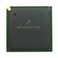
IC MPU 32BIT 56MHZ PPC 388-PBGA
Manufacturer
Freescale Semiconductor
Series
MPC5xxr
Datasheet
1.MPC561MZP56.pdf
(1420 pages)
Specifications of MPC562MZP56
Core Processor
PowerPC
Core Size
32-Bit
Speed
56MHz
Connectivity
CAN, EBI/EMI, SCI, SPI, UART/USART
Peripherals
POR, PWM, WDT
Number Of I /o
64
Program Memory Type
ROMless
Ram Size
32K x 8
Voltage - Supply (vcc/vdd)
2.5 V ~ 2.7 V
Data Converters
A/D 32x10b
Oscillator Type
External
Operating Temperature
-40°C ~ 125°C
Package / Case
388-BGA
Processor Series
MPC5xx
Core
PowerPC
Data Bus Width
32 bit
Data Ram Size
8 KB
Interface Type
SCI, SPI, UART
Maximum Clock Frequency
40 MHz
Number Of Programmable I/os
56
Number Of Timers
22
Operating Supply Voltage
2.6 V to 5 V
Maximum Operating Temperature
+ 85 C
Mounting Style
SMD/SMT
Minimum Operating Temperature
- 40 C
On-chip Adc
2 (10 bit, 32 Channel)
For Use With
MPC564EVB - KIT EVAL FOR MPC561/562/563/564
Lead Free Status / RoHS Status
Request inventory verification / Request inventory verification
Eeprom Size
-
Program Memory Size
-
Lead Free Status / Rohs Status
No
Available stocks
Company
Part Number
Manufacturer
Quantity
Price
Company:

Part Number:
MPC562MZP56
Manufacturer:
FREESCAL
Quantity:
204
Company:
Part Number:
MPC562MZP56
Manufacturer:
Freescale Semiconductor
Quantity:
10 000
Part Number:
MPC562MZP56
Manufacturer:
FREESCALE
Quantity:
20 000
Company:
Part Number:
MPC562MZP56R2
Manufacturer:
RFT
Quantity:
1 441
Company:
Part Number:
MPC562MZP56R2
Manufacturer:
Freescale Semiconductor
Quantity:
10 000


6-11
6-12
6-13
6-14
6-15
6-16
6-17
6-18
6-19
6-20
6-21
6-22
6-23
6-24
6-25
6-26
7-1
7-2
7-3
7-4
7-5
8-1
8-2
8-3
8-4
8-5
8-6
8-7
8-8
8-9
8-10
8-11
8-12
8-13
9-1
9-2
9-3
9-4
9-5
Freescale Semiconductor
Table
Number
Multi-Level Reservation Control Pin Configuration .............................................................. 6-28
SIU Interrupt Controller – Bit Acronym Definitions.............................................................. 6-31
Data Direction Control............................................................................................................ 6-48
Reset Action Taken for Each Reset Cause ............................................................................... 7-4
Reset Configuration Word and Data Corruption/Coherency.................................................... 7-4
Reset Status Register Bit Descriptions ..................................................................................... 7-5
Reset Configuration Options .................................................................................................... 7-7
RCW Bit Descriptions ............................................................................................................ 7-11
Reset Clocks Source Configuration .......................................................................................... 8-9
TMBCLK Divisions ............................................................................................................... 8-10
Status of Clock Source............................................................................................................ 8-16
Power Supplies ....................................................................................................................... 8-21
KAPWR Registers and Key Registers.................................................................................... 8-26
SCCR Bit Descriptions ........................................................................................................... 8-30
COM and CQDS Bits Functionality ....................................................................................... 8-33
MPC561/MPC563 BIU Signals................................................................................................ 9-4
Data Bus Requirements For Read Cycles............................................................................... 9-31
Data Bus Contents for Write Cycles....................................................................................... 9-32
Priority Between Internal and External Masters over External Bus ....................................... 9-36
4 Word Burst Length and Order ............................................................................................. 9-38
IMMR Bit Descriptions ......................................................................................................... 6-29
EMCR Bit Descriptions ......................................................................................................... 6-30
SYPCR Bit Descriptions........................................................................................................ 6-38
SWSR Bit Descriptions ......................................................................................................... 6-39
TESR Bit Descriptions........................................................................................................... 6-39
TBSCR Bit Descriptions........................................................................................................ 6-42
RTCSC Bit Descriptions........................................................................................................ 6-43
PISCR Bit Descriptions ......................................................................................................... 6-44
PITC Bit Descriptions............................................................................................................ 6-45
PIT Bit Descriptions .............................................................................................................. 6-45
SGPIODT1 Bit Descriptions ................................................................................................. 6-46
SGPIODT2 Bit Descriptions ................................................................................................. 6-47
SGPIOCR Bit Descriptions ................................................................................................... 6-48
Power Mode Control Bit Settings .......................................................................................... 8-17
Power Mode Descriptions...................................................................................................... 8-17
Power Mode Wake-Up Operation ......................................................................................... 8-18
PLPRCR Bit Descriptions ..................................................................................................... 8-34
COLIR Bit Descriptions ........................................................................................................ 8-36
VSRMCR Bit Descriptions.................................................................................................... 8-37
MPC561/MPC563 Reference Manual, Rev. 1.2
Tables
Title
Number
Page
lxv
Related parts for MPC562MZP56
Image
Part Number
Description
Manufacturer
Datasheet
Request
R

Part Number:
Description:
Mpc562 32 Bit Powerpc Microcontroller
Manufacturer:
Freescale Semiconductor, Inc
Datasheet:

Part Number:
Description:
MPC5 1K0 5%
Manufacturer:
TE Connectivity
Datasheet:


Part Number:
Description:
MPC5 500R 5%
Manufacturer:
TE Connectivity
Datasheet:

Part Number:
Description:
MPC5 5K0 5%
Manufacturer:
Tyco Electronics
Datasheet:
Part Number:
Description:
MPC5 5R0 5%
Manufacturer:
Tyco Electronics
Datasheet:
Part Number:
Description:
MPC5 50K 5%
Manufacturer:
Tyco Electronics
Datasheet:
Part Number:
Description:
Manufacturer:
Freescale Semiconductor, Inc
Datasheet:
Part Number:
Description:
Manufacturer:
Freescale Semiconductor, Inc
Datasheet:
Part Number:
Description:
Manufacturer:
Freescale Semiconductor, Inc
Datasheet:
Part Number:
Description:
Manufacturer:
Freescale Semiconductor, Inc
Datasheet:
Part Number:
Description:
Manufacturer:
Freescale Semiconductor, Inc
Datasheet: