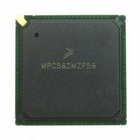
MPC562MZP56 Freescale Semiconductor, MPC562MZP56 Datasheet - Page 642

MPC562MZP56
Manufacturer Part Number
MPC562MZP56
Description
IC MPU 32BIT 56MHZ PPC 388-PBGA
Manufacturer
Freescale Semiconductor
Series
MPC5xxr
Datasheet
1.MPC561MZP56.pdf
(1420 pages)
Specifications of MPC562MZP56
Core Processor
PowerPC
Core Size
32-Bit
Speed
56MHz
Connectivity
CAN, EBI/EMI, SCI, SPI, UART/USART
Peripherals
POR, PWM, WDT
Number Of I /o
64
Program Memory Type
ROMless
Ram Size
32K x 8
Voltage - Supply (vcc/vdd)
2.5 V ~ 2.7 V
Data Converters
A/D 32x10b
Oscillator Type
External
Operating Temperature
-40°C ~ 125°C
Package / Case
388-BGA
Processor Series
MPC5xx
Core
PowerPC
Data Bus Width
32 bit
Data Ram Size
8 KB
Interface Type
SCI, SPI, UART
Maximum Clock Frequency
40 MHz
Number Of Programmable I/os
56
Number Of Timers
22
Operating Supply Voltage
2.6 V to 5 V
Maximum Operating Temperature
+ 85 C
Mounting Style
SMD/SMT
Minimum Operating Temperature
- 40 C
On-chip Adc
2 (10 bit, 32 Channel)
For Use With
MPC564EVB - KIT EVAL FOR MPC561/562/563/564
Lead Free Status / RoHS Status
Request inventory verification / Request inventory verification
Eeprom Size
-
Program Memory Size
-
Lead Free Status / Rohs Status
No
Available stocks
Company
Part Number
Manufacturer
Quantity
Price
Company:
Part Number:
MPC562MZP56
Manufacturer:
FREESCAL
Quantity:
204
Company:
Part Number:
MPC562MZP56
Manufacturer:
Freescale Semiconductor
Quantity:
10 000
Part Number:
MPC562MZP56
Manufacturer:
FREESCALE
Quantity:
20 000
Company:
Part Number:
MPC562MZP56R2
Manufacturer:
RFT
Quantity:
1 441
Company:
Part Number:
MPC562MZP56R2
Manufacturer:
Freescale Semiconductor
Quantity:
10 000
- Current page: 642 of 1420
- Download datasheet (11Mb)
Queued Serial Multi-Channel Module
Refer to
15.6.3
Seven pins are associated with the QSPI. When not needed by the QSPI, they can be configured for
general-purpose I/O.
determines whether the pins are designated as input or output. The user must initialize DDRQS for the
QSPI to function correctly.
15-24
Bits
4:7
0
1
2
3
The PCS0 bit represents the dual-function PCS0/SS.
1
PCS[3:0] Peripheral chip selects. Use peripheral chip-select bits to select an external device for serial data transfer. More
CONT
CONT
BITSE
Name
CONT
DSCK
MSB
DT
Section 15.6.5, “Master Mode
—
0
QSPI Pins
Continue
0 Control of chip selects returned to PORTQS after transfer is complete.
1 Peripheral chip selects remain asserted after transfer is complete.
Bits per transfer enable
0 Eight bits
1 Number of bits set in BITS field of SPCR0.
Delay after transfer
0 Delay after transfer is 17 ÷ f
1 SPCR1 DTL[7:0] specifies delay after transfer PCS valid to SCK.
PCS to SCK Delay
0 PCS valid to SCK delay is one-half SCK.
1 SPCR1 DSCKL[6:0] specifies delay from PCS valid to SCK.
than one peripheral chip select may be activated at a time, and more than one peripheral chip can be connected
to each PCS pin, provided proper fanout is observed. PCS0 shares a pin with the slave select (SS) signal, which
initiates slave mode serial transfer. If SS is taken low when the QSPI is in master mode, a mode fault occurs.
BITSE
BITSE
Command Control
—
Table 15-20
1
Figure 15-17. CR[0:F] — Command RAM 0x30 51C0, 0x30 51DF
Table 15-19. Command RAM Bit Descriptions
MPC561/MPC563 Reference Manual, Rev. 1.2
DT
DT
—
2
identifies the QSPI pins and their functions. Register DDRQS
Operation” for more information on the command RAM.
SYS
.
DSCK
DSCK
—
3
Description
PCS3
PCS3
—
4
Peripheral Chip Select
PCS2
PCS2
—
5
PCS1
PCS1
—
6
Freescale Semiconductor
PCS0
PCS0
LSB
—
7
1
1
Related parts for MPC562MZP56
Image
Part Number
Description
Manufacturer
Datasheet
Request
R
Part Number:
Description:
Mpc562 32 Bit Powerpc Microcontroller
Manufacturer:
Freescale Semiconductor, Inc
Datasheet:

Part Number:
Description:
MPC5 1K0 5%
Manufacturer:
TE Connectivity
Datasheet:

Part Number:
Description:
MPC5 500R 5%
Manufacturer:
TE Connectivity
Datasheet:

Part Number:
Description:
MPC5 5K0 5%
Manufacturer:
Tyco Electronics
Datasheet:

Part Number:
Description:
MPC5 5R0 5%
Manufacturer:
Tyco Electronics
Datasheet:

Part Number:
Description:
MPC5 50K 5%
Manufacturer:
Tyco Electronics
Datasheet:
Part Number:
Description:
Manufacturer:
Freescale Semiconductor, Inc
Datasheet:
Part Number:
Description:
Manufacturer:
Freescale Semiconductor, Inc
Datasheet:
Part Number:
Description:
Manufacturer:
Freescale Semiconductor, Inc
Datasheet:
Part Number:
Description:
Manufacturer:
Freescale Semiconductor, Inc
Datasheet:
Part Number:
Description:
Manufacturer:
Freescale Semiconductor, Inc
Datasheet:


