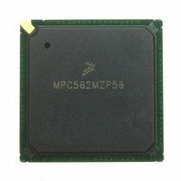
MPC562MZP56 Freescale Semiconductor, MPC562MZP56 Datasheet - Page 547

MPC562MZP56
Manufacturer Part Number
MPC562MZP56
Description
IC MPU 32BIT 56MHZ PPC 388-PBGA
Manufacturer
Freescale Semiconductor
Series
MPC5xxr
Datasheet
1.MPC561MZP56.pdf
(1420 pages)
Specifications of MPC562MZP56
Core Processor
PowerPC
Core Size
32-Bit
Speed
56MHz
Connectivity
CAN, EBI/EMI, SCI, SPI, UART/USART
Peripherals
POR, PWM, WDT
Number Of I /o
64
Program Memory Type
ROMless
Ram Size
32K x 8
Voltage - Supply (vcc/vdd)
2.5 V ~ 2.7 V
Data Converters
A/D 32x10b
Oscillator Type
External
Operating Temperature
-40°C ~ 125°C
Package / Case
388-BGA
Processor Series
MPC5xx
Core
PowerPC
Data Bus Width
32 bit
Data Ram Size
8 KB
Interface Type
SCI, SPI, UART
Maximum Clock Frequency
40 MHz
Number Of Programmable I/os
56
Number Of Timers
22
Operating Supply Voltage
2.6 V to 5 V
Maximum Operating Temperature
+ 85 C
Mounting Style
SMD/SMT
Minimum Operating Temperature
- 40 C
On-chip Adc
2 (10 bit, 32 Channel)
For Use With
MPC564EVB - KIT EVAL FOR MPC561/562/563/564
Lead Free Status / RoHS Status
Request inventory verification / Request inventory verification
Eeprom Size
-
Program Memory Size
-
Lead Free Status / Rohs Status
No
Available stocks
Company
Part Number
Manufacturer
Quantity
Price
Company:
Part Number:
MPC562MZP56
Manufacturer:
FREESCAL
Quantity:
204
Company:
Part Number:
MPC562MZP56
Manufacturer:
Freescale Semiconductor
Quantity:
10 000
Part Number:
MPC562MZP56
Manufacturer:
FREESCALE
Quantity:
20 000
Company:
Part Number:
MPC562MZP56R2
Manufacturer:
RFT
Quantity:
1 441
Company:
Part Number:
MPC562MZP56R2
Manufacturer:
Freescale Semiconductor
Quantity:
10 000
- Current page: 547 of 1420
- Download datasheet (11Mb)
to the LOCK and FLIP bits of the module configuration register. This will be described in
“Switching Between Legacy and Enhanced Modes of
14.2.4
The heart of the QADC is its conversion command word (CCW) queues. This is where the module is
programmed to convert a particular channel according to a particular requirement. The queues are created
by writing CCWs into the CCW table in the register memory. The queues are controlled by the three
control registers, and their status can be read from the two status registers. As conversions are completed
the digital value is written into the result word table.
word table.
14.2.5
The QADC can use from one to four 8-input external multiplexer chips to expand the number of analog
signals that may be converted. The externally multiplexed channels are automatically selected from the
Freescale Semiconductor
0x27E (CCW63)
0x200 (CCW0)
P = Pause Until Next Trigger
REF = Use Alternate Reference Voltage
IST = Input Sample Time
CHAN = Channel Number and End_of_Queue Code
Using the Queue and Result Word Table
External Multiplexing
BQ2
msb
NOTE 1: These offsets must be added to the module base address: A = 0x30 4800 or B = 0x30 4C00
6
P REF IST
10-bit Conversion
Conversion Command
Command Word
Word (CCW) Table
(CCW) Format
7
Begin Queue 1
End of Queue 1
Begin Queue 2
End of Queue 2
Figure 14-2. CCW Queue and Result Table Block Diagram
8
9
CHAN
MPC561/MPC563 Reference Manual, Rev. 1.2
15
lsb
Analog to Digital
Channel Select,
Sample, Hold,
Conversion
A/D Converter
and
Right Justified, Unsigned Result Format
Figure 14-2
msb
0 0
0
S
Left Justified, Unsigned Result Format
0
0
Operation.”
Left Justified, Signed Result Format
1
0 0 0
in Three Different 16-bit Formats
Result
Result
0
Software Readable
shows the CCW queue and the result
10-bit Result is
Result Word Table
7 8
7 8
7 8
Result
0 0
0 0
QADC64E Enhanced Mode Operation
0 0 0
0
0 0
lsb
15
15
15
0
0
Result 0
Result 63
Address Offsets:
0x280-0x2FF
0x300-0x37F
Section 14.3.1.3,
0x380-0x3FF
S = Sign bit
1
1
1
14-5
Related parts for MPC562MZP56
Image
Part Number
Description
Manufacturer
Datasheet
Request
R
Part Number:
Description:
Mpc562 32 Bit Powerpc Microcontroller
Manufacturer:
Freescale Semiconductor, Inc
Datasheet:

Part Number:
Description:
MPC5 1K0 5%
Manufacturer:
TE Connectivity
Datasheet:

Part Number:
Description:
MPC5 500R 5%
Manufacturer:
TE Connectivity
Datasheet:

Part Number:
Description:
MPC5 5K0 5%
Manufacturer:
Tyco Electronics
Datasheet:

Part Number:
Description:
MPC5 5R0 5%
Manufacturer:
Tyco Electronics
Datasheet:

Part Number:
Description:
MPC5 50K 5%
Manufacturer:
Tyco Electronics
Datasheet:
Part Number:
Description:
Manufacturer:
Freescale Semiconductor, Inc
Datasheet:
Part Number:
Description:
Manufacturer:
Freescale Semiconductor, Inc
Datasheet:
Part Number:
Description:
Manufacturer:
Freescale Semiconductor, Inc
Datasheet:
Part Number:
Description:
Manufacturer:
Freescale Semiconductor, Inc
Datasheet:
Part Number:
Description:
Manufacturer:
Freescale Semiconductor, Inc
Datasheet:


