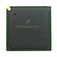
MPC562MZP56 Freescale Semiconductor, MPC562MZP56 Datasheet - Page 431

MPC562MZP56
Manufacturer Part Number
MPC562MZP56
Description
IC MPU 32BIT 56MHZ PPC 388-PBGA
Manufacturer
Freescale Semiconductor
Series
MPC5xxr
Datasheet
1.MPC561MZP56.pdf
(1420 pages)
Specifications of MPC562MZP56
Core Processor
PowerPC
Core Size
32-Bit
Speed
56MHz
Connectivity
CAN, EBI/EMI, SCI, SPI, UART/USART
Peripherals
POR, PWM, WDT
Number Of I /o
64
Program Memory Type
ROMless
Ram Size
32K x 8
Voltage - Supply (vcc/vdd)
2.5 V ~ 2.7 V
Data Converters
A/D 32x10b
Oscillator Type
External
Operating Temperature
-40°C ~ 125°C
Package / Case
388-BGA
Processor Series
MPC5xx
Core
PowerPC
Data Bus Width
32 bit
Data Ram Size
8 KB
Interface Type
SCI, SPI, UART
Maximum Clock Frequency
40 MHz
Number Of Programmable I/os
56
Number Of Timers
22
Operating Supply Voltage
2.6 V to 5 V
Maximum Operating Temperature
+ 85 C
Mounting Style
SMD/SMT
Minimum Operating Temperature
- 40 C
On-chip Adc
2 (10 bit, 32 Channel)
For Use With
MPC564EVB - KIT EVAL FOR MPC561/562/563/564
Lead Free Status / RoHS Status
Request inventory verification / Request inventory verification
Eeprom Size
-
Program Memory Size
-
Lead Free Status / Rohs Status
No
Available stocks
Company
Part Number
Manufacturer
Quantity
Price
Company:
Part Number:
MPC562MZP56
Manufacturer:
FREESCAL
Quantity:
204
Company:
Part Number:
MPC562MZP56
Manufacturer:
Freescale Semiconductor
Quantity:
10 000
Part Number:
MPC562MZP56
Manufacturer:
FREESCALE
Quantity:
20 000
Company:
Part Number:
MPC562MZP56R2
Manufacturer:
RFT
Quantity:
1 441
Company:
Part Number:
MPC562MZP56R2
Manufacturer:
Freescale Semiconductor
Quantity:
10 000
- Current page: 431 of 1420
- Download datasheet (11Mb)
Freescale Semiconductor
17:19
20:21
Bits
0:16
22
23
24
25
26
27
28
29
WEBS
TBDIP
LBDIP
Name
SETA
SST
WP
BA
PS
BL
AT
—
Base address. These bits are compared to the corresponding unmasked address signals among
ADDR[0:16] to determine if a memory bank controlled by the memory controller is being
accessed by an internal bus master. (The address types are also compared.) These bits are used
in conjunction with the AM[0:16] bits in the OR.
Address type. This field can be used to require accesses of the memory bank to be limited to a
certain address space type. These bits are used in conjunction with the ATM bits in the OR. Note
that the address type field uses only AT[0:2] and does not need AT3 to define the memory type
space. For a full definition of address types, refer to
Port size
00 32-bit port
01 8-bit port
10 16-bit port
11 Reserved
Short Setup Time – This field specifies the setup time required for this memory region.
0 Normal setup time (like the MPC555)
1 Short Setup Time selected
Note that an external burst access with short setup timing will corrupt any USIU register
load/store if SCCR[EBDF] is not 0b00. Refer to
Write protect. An attempt to write to the range of addresses specified in a base address register
that has this bit set can cause the TEA signal to be asserted by the bus-monitor logic (if enabled),
causing termination of this cycle.
0 Both read and write accesses are allowed
1 Only read accesses are allowed. The CSx signal and TA are not asserted by the memory
Reserved
Burst Length – This field specifies the maximum number of words that may comprise a burst
access for this memory region. This field has an effect only in the case when the burst accesses
are initiated by the USIU (SIUMCR[BURST_EN] =1).
0 Burst access of up to 4 words
1 Burst access of up to 8 words
Write-enable/byte-select. This bit controls the functionality of the WE/BE pads.
0 The WE/BE pads operate as WE
1 The WE/BE pads operate as BE
Toggle-burst data in progress. TBDIP determines how long the BDIP strobe will be asserted for
each data beat in the burst cycles.
Late-burst-data-in-progress (LBDIP). This bit determines the timing of the first assertion of the
BDIP signal in burst cycles.
NOTE: Do not set both LBDIP and TBDIP bits in a region’s base registers; behavior in such cases
is unpredictable.
0 Normal timing for BDIP assertion (asserts one clock after negation of TS)
1 Late timing for BDIP assertion (asserts after the programmed number of wait states)
External transfer acknowledge
0 TA generated internally by memory controller
1 TA generated by external logic. Note that programming the timing of CS/WE/OE strobes may
controller on write cycles to this memory bank. WPER is set in the MSTAT register if a write to
this memory bank is attempted
have no meaning when this bit is set
MPC561/MPC563 Reference Manual, Rev. 1.2
Table 10-8. BR0–BR3 Bit Descriptions
Description
Table
Section 9.5.8.6, “Address
8-9.
Types.”
Memory Controller
10-33
Related parts for MPC562MZP56
Image
Part Number
Description
Manufacturer
Datasheet
Request
R
Part Number:
Description:
Mpc562 32 Bit Powerpc Microcontroller
Manufacturer:
Freescale Semiconductor, Inc
Datasheet:

Part Number:
Description:
MPC5 1K0 5%
Manufacturer:
TE Connectivity
Datasheet:

Part Number:
Description:
MPC5 500R 5%
Manufacturer:
TE Connectivity
Datasheet:

Part Number:
Description:
MPC5 5K0 5%
Manufacturer:
Tyco Electronics
Datasheet:

Part Number:
Description:
MPC5 5R0 5%
Manufacturer:
Tyco Electronics
Datasheet:

Part Number:
Description:
MPC5 50K 5%
Manufacturer:
Tyco Electronics
Datasheet:
Part Number:
Description:
Manufacturer:
Freescale Semiconductor, Inc
Datasheet:
Part Number:
Description:
Manufacturer:
Freescale Semiconductor, Inc
Datasheet:
Part Number:
Description:
Manufacturer:
Freescale Semiconductor, Inc
Datasheet:
Part Number:
Description:
Manufacturer:
Freescale Semiconductor, Inc
Datasheet:
Part Number:
Description:
Manufacturer:
Freescale Semiconductor, Inc
Datasheet:


