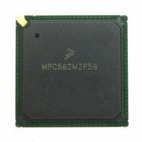
MPC562MZP56 Freescale Semiconductor, MPC562MZP56 Datasheet - Page 1210

MPC562MZP56
Manufacturer Part Number
MPC562MZP56
Description
IC MPU 32BIT 56MHZ PPC 388-PBGA
Manufacturer
Freescale Semiconductor
Series
MPC5xxr
Datasheet
1.MPC561MZP56.pdf
(1420 pages)
Specifications of MPC562MZP56
Core Processor
PowerPC
Core Size
32-Bit
Speed
56MHz
Connectivity
CAN, EBI/EMI, SCI, SPI, UART/USART
Peripherals
POR, PWM, WDT
Number Of I /o
64
Program Memory Type
ROMless
Ram Size
32K x 8
Voltage - Supply (vcc/vdd)
2.5 V ~ 2.7 V
Data Converters
A/D 32x10b
Oscillator Type
External
Operating Temperature
-40°C ~ 125°C
Package / Case
388-BGA
Processor Series
MPC5xx
Core
PowerPC
Data Bus Width
32 bit
Data Ram Size
8 KB
Interface Type
SCI, SPI, UART
Maximum Clock Frequency
40 MHz
Number Of Programmable I/os
56
Number Of Timers
22
Operating Supply Voltage
2.6 V to 5 V
Maximum Operating Temperature
+ 85 C
Mounting Style
SMD/SMT
Minimum Operating Temperature
- 40 C
On-chip Adc
2 (10 bit, 32 Channel)
For Use With
MPC564EVB - KIT EVAL FOR MPC561/562/563/564
Lead Free Status / RoHS Status
Request inventory verification / Request inventory verification
Eeprom Size
-
Program Memory Size
-
Lead Free Status / Rohs Status
No
Available stocks
Company
Part Number
Manufacturer
Quantity
Price
Company:
Part Number:
MPC562MZP56
Manufacturer:
FREESCAL
Quantity:
204
Company:
Part Number:
MPC562MZP56
Manufacturer:
Freescale Semiconductor
Quantity:
10 000
Part Number:
MPC562MZP56
Manufacturer:
FREESCALE
Quantity:
20 000
Company:
Part Number:
MPC562MZP56R2
Manufacturer:
RFT
Quantity:
1 441
Company:
Part Number:
MPC562MZP56R2
Manufacturer:
Freescale Semiconductor
Quantity:
10 000
- Current page: 1210 of 1420
- Download datasheet (11Mb)
TPU3 ROM Functions
active, these performance figures will be degraded; however, the scheduler assures that the worst-case
latency in any TPU3 application can be closely approximated. TPU3 reference manual guidelines and
information given in the SIOP-state timing table should be used to perform an analysis on any proposed
TPU3 application that appears to approach the TPU’s performance limits.
D.20.3.1
XFER_SIZE is normally programmed to be in the 1- to 16-bit range to match the size of SIOP_DATA, and
has thus been shown as a 5-bit value in the host interface diagram. However, the TPU3 actually uses all 16
bits of the XFER_SIZE parameter when loading BIT_COUNT. In some unusual circumstances this can be
used to an advantage. If an input device is producing a data stream of greater than 16 bits then manipulation
of XFER_SIZE will allow selective capturing of the data. In clock-only mode, the extended XFER_SIZE
can be used to generate up to 0xFFFF clocks.
D.20.3.2
As stated above, the TPU3 does not “justify” the data position in SIOP_DATA. Therefore, in the case of a
byte transfer, the data output will be sourced from one byte and the data input will shift into the other byte.
This is true for all data sizes except 16 bits, in which case the full SIOP_DATA register is used for both
data output and input.
D.20.3.3
In the example given in
synchronous with the relevant clock edge and it is assumed that the data input is latched exactly on the
opposite clock edge. This is the simplest way to show the examples, but is not strictly true. Since the TPU3
is a multi-tasking system, and the data channels are manipulated directly by microcode software while
servicing the clock edge, there is a finite delay between the relevant clock edge and the data-out being valid
or the data-in being latched. This delay is equivalent to the latency in servicing the clock channel due to
other TPU3 activity and is shown as ‘Td’ in the timing diagram. Td is the delay between the clock edge
and the next output data being valid and also the delay between the opposite clock edge and the input data
being read. For the vast majority of applications, the delay Td will not present a problem and can be
ignored. Only for a system which heavily loads the TPU3 should the worst case latency be calculated for
D-58
1
Execution times do not include the time slot transition time (TST = 10 or 14 RCPU clocks).
State Number and Name
XFER_SIZE Greater Than 16
Data Positioning
Data Timing
S2 DATA_OUT
S1 SIOP_INIT
S3 DATA_IN
HSQ = X0
HSQ = X0
HSQ = 0X
X1
X1
1X
Figure
D-33, the data output transitions are shown as being completely
MPC561/MPC563 Reference Manual, Rev. 1.2
Table D-4. SIOP State Timing
Max. RCPU Clock Cycles
28
38
14
24
14
28
1
Number of RAM Accesses by TPU3
Freescale Semiconductor
7
7
4
4
4
6
Related parts for MPC562MZP56
Image
Part Number
Description
Manufacturer
Datasheet
Request
R
Part Number:
Description:
Mpc562 32 Bit Powerpc Microcontroller
Manufacturer:
Freescale Semiconductor, Inc
Datasheet:

Part Number:
Description:
MPC5 1K0 5%
Manufacturer:
TE Connectivity
Datasheet:

Part Number:
Description:
MPC5 500R 5%
Manufacturer:
TE Connectivity
Datasheet:

Part Number:
Description:
MPC5 5K0 5%
Manufacturer:
Tyco Electronics
Datasheet:

Part Number:
Description:
MPC5 5R0 5%
Manufacturer:
Tyco Electronics
Datasheet:

Part Number:
Description:
MPC5 50K 5%
Manufacturer:
Tyco Electronics
Datasheet:
Part Number:
Description:
Manufacturer:
Freescale Semiconductor, Inc
Datasheet:
Part Number:
Description:
Manufacturer:
Freescale Semiconductor, Inc
Datasheet:
Part Number:
Description:
Manufacturer:
Freescale Semiconductor, Inc
Datasheet:
Part Number:
Description:
Manufacturer:
Freescale Semiconductor, Inc
Datasheet:
Part Number:
Description:
Manufacturer:
Freescale Semiconductor, Inc
Datasheet:


